Skip to main content
Mobile menu
Solutions
Octopart Discover
Go beyond part search to discover viable solutions, evaluate tradeoffs, and make better decisions earlier
Altium Develop
Design advanced PCBs in Altium Designer, working independently or connecting reviewers, sourcing data, and release coordination when needed
Altium Agile Teams
Bring structure to multidisciplinary electronics development and collaboration without sacrificing speed
Altium Agile Enterprise
Connect context from intent through release with an intelligent, governed, extensible platform
Resources & Support
Free Altium 365 Tools
Gerber Compare
Online PCB Viewer
Resources & Support
Learning Hub
Support Center
Documentation
Webinars
Altium Community
Forum
Bug Crunch
Ideas
Education & Training
Student Lab
Free access to professional PCB design software, training, and learning resources for students
Educator Center
A comprehensive education platform providing curriculum, software, training, and classroom resources for educators
Altium Education Curriculum
Free college- and university-level PCB design curriculum designed to prepare students for real-world engineering careers
Altium Professional Training
Flexible on-demand and instructor-led training courses that help engineers build and advance their PCB design skills
Search Open
Search
Search Close
Sign In
신호 무결성
Main menu
블로그 홈
PCB 디자인
팀 공동 작업
컴포넌트 생성
설계 데이터 관리
설계 산출물
ECAD/MCAD
HDI 설계
고속 디자인
멀티 보드
PCB 레이아웃
PCB 라우팅
공급망
전력 무결성
RF 설계
리지드 플렉스
회로도 캡처
신호 무결성
시뮬레이션 / 분석
소프트웨어
Develop
Discover
Agile
Altium 365
Altium Designer
리소스
프로그램
Altium Academy
엔지니어링 뉴스
가이드 북
뉴스레터
팟 캐스트
프로젝트
교육 과정
웹 세미나
하얀 종이
Learning Hub
신호 무결성
신호 무결성
PCB 설계 및 신호 무결성에 대해 더 알아보려면 리소스 라이브러리를 살펴보세요.
신호 무결성이란 무엇인가요?
PCB 설계 기초
Altium의 xSignals
신호 무결성 자극 설계 규칙
신호 무결성 분석의 기초
Overview
가이드북
Tech Docs
All Content
Filter
검색됨
Sort by
최신순
인기순
제목 (A-Z)
제목 (Z-A)
역할
전기 엔지니어
PCB 설계 엔지니어
소프트웨어
개발하다
애자일
Altium Designer
Altium 365
Octopart
콘텐츠 유형
가이드북
팟캐스트
백서
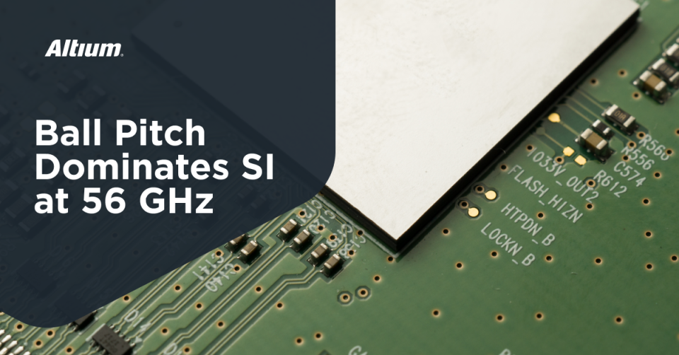
224G-PAM4 및 448G에서 BGA 핀 피치가 신호 무결성에 미치는 영향
9 min
Blog
PCB 설계 엔지니어
PCB 산업은 제조 및 신호 무결성 측면에서 항상 반도체 패키징보다 뒤처져 있는 것 같습니다. 산업이 데모에서 생산으로 넘어가는 224G 인터페이스를
문서 읽기
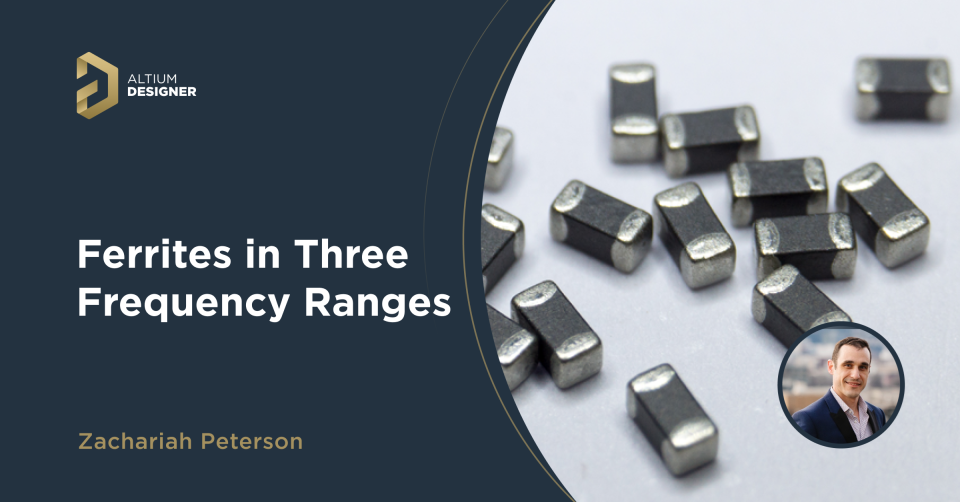
페라이트 비드 사용을 위한 세 가지 주파수 범위
7 min
Blog
전기 엔지니어
PCB 설계 엔지니어
세 가지 운영 시나리오는 페라이트 비드 임피던스에 대한 세 가지 중요한 주파수 범위와 디지털 시스템에서의 노이즈에 미치는 영향을 보여줍니다.
문서 읽기
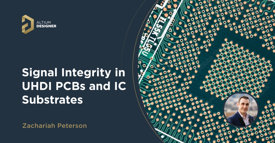
얇은 초고밀도(HDI) PCB 레이어에서의 신호 무결성
10 min
Blog
PCB 설계 엔지니어
PCB 신호 무결성은 HDI 및 초고밀도 HDI PCB에서 사용되는 초박형 PCB 층에서 발생하는 현상을 살펴볼 때 변하기 시작합니다.
문서 읽기
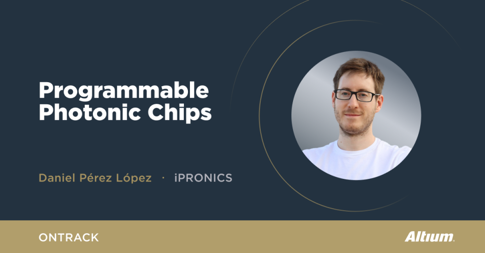
포토닉스, 차세대 통신 프로세서
25 min
Podcasts
PCB 설계 엔지니어
포토닉 아이폰과 스마트폰이 필요한가요? 오늘 우리는 매우 흥미로운 주제를 가지고 있습니다. iPRONICS의 CTO이자 공동 창립자인 Daniel Pérez López와 함께합니다. 프로그래밍 가능한 포토닉스입니다.
문서 읽기
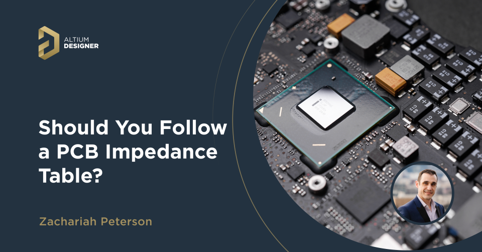
PCB 임피던스 테이블 읽는 방법
5 min
Blog
PCB 설계 엔지니어
PCB 임피던스 테이블은 설계자가 재료나 스택업을 선택하지 않고 특정 레이어에서의 트레이스 임피던스 값을 보여줍니다.
문서 읽기
PCB 및 패키지 디자인을 위한 224G PAM-4 채널
11 min
Blog
전기 엔지니어
224G PAM-4을 통한 다음 인터페이스 및 패키징 이정표가 도래했습니다. 이 채널들이 어떻게 광대역 신호 무결성을 제공하도록 설계될 수 있는지에 대해 알아보겠습니다.
문서 읽기
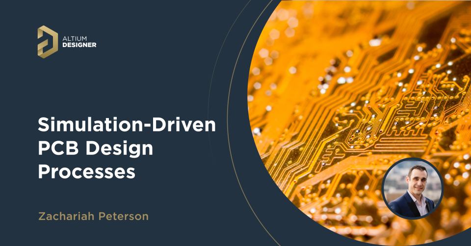
시뮬레이션 주도 설계는 PCB의 신호 문제 등을 해결할 수 있습니다
8 min
Blog
시뮬레이션 엔지니어
전자 산업이나 연구 분야에서 일한다면, 시뮬레이션이 일상의 일부일 가능성이 있습니다. 더 간단한 시스템은 직관을 통해 설계될 수 있으며 설계가 완료된
문서 읽기
Pagination
First page
« First
Previous page
‹‹
Page
3
현재 페이지
4
Page
5
Page
6
Page
7
Page
8
Next page
››
Last page
Last »