Skip to main content
Mobile menu
Discover
Develop
Agile
Resources & Support
Free Altium 365 Tools
Gerber Compare
Online PCB Viewer
Resources & Support
Learning Hub
Support Center
Documentation
Webinars
Altium Community
Forum
Bug Crunch
Ideas
Education
Student Lab
Educator Center
Altium Education Curriculum
Search Open
Search
Search Close
Sign In
Main menu
Home
PCB Design
Collaboration
Component Creation
Data Management
Design Outputs
ECAD/MCAD
HDI Design
High Speed Design
Multi-Board
PCB Layout
PCB Routing
PCB Supply Chain
Power Integrity
RF Design
Rigid Flex
Schematic Capture
Signal Integrity
Simulation
Software
Develop
Discover
Agile
Altium 365
Altium Designer
Education
Programs
Altium Academy
Engineering News
Guide Books
Newsletters
Podcasts
Projects
Training Courses
Webinars
Whitepapers
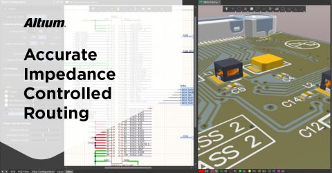
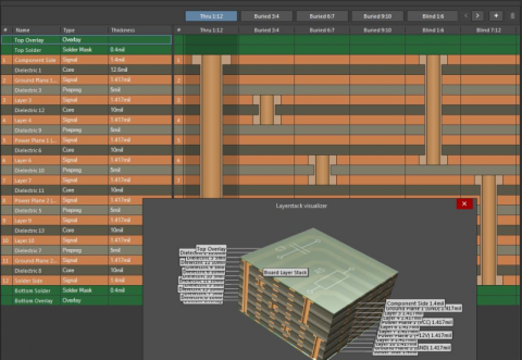
How to Ensure Impedance Control in PCB Routing
Impedance control in PCB designs can refer to two different practices depending on who you're speaking with. PCB manufacturers provide impedance control as a service to customers who want to manufacture a high-speed digital system or an RF design. In contrast, PCB designers use the term to refer to intentional material selection and specification for their PCB stack-up, often without consideration of what materials a manufacturer might have
Read Article
How to Design and Route Your RF Filter PCB Layout
RF PCBs and mixed-signal systems are challenging for many designers. Careful attention must be paid to the PCB stackup design, process for designing transmission lines, placement of components, and floorplanning the PCB layout to ensure predictable return path. Many RF PCB layout designs will include printed elements, like an RF filter, antenna, isolation structures, and unique waveguide geometries. RF systems can make copious use of RF filters
Read Article
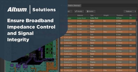
What is the High-Speed Signal Frequency Range and Bandwidth?
The high speed signal frequency range and bandwidth will affect signal integrity. Use the best design tools that can accommodate broadband signals in your PCB.
Read Article
PCB Heat Sinks: Thermal Pad vs. Paste in Your Circuit Board Design
Using thermal pads vs paste is an important decision when deciding how to best attach a heat sink to a power-hungry component like a CPU. Each of these materials gives the important benefit of heat transfer and reduced temperature, but there are other points to be considered when using a heat sink with a thermal pad or thermal paste. Assembly houses also need to know which option a design will use, requiring that clear documentation be provided
Read Article
How to Make Copper-Clad Boards With the Best PCB Layout Software
Some designers prefer to build their own prototypes in their home or company lab as it gives them a firsthand view of potential quality problems in their boards. While designers can go this route if they’re comfortable using etchants and cleaning solutions needed to remove copper from PCB laminates, they’ll need design tools to create their etching stencils. An at-home designer will need to procure PCB copper boards to use for etching and create
Read Article
How to Design Coplanar Waveguide with Ground in Your PCB
RF designs that run at high frequency need high isolation from digital components, power subsystems, and external sources of noise that can degrade signal quality. One option in many RF designs is coplanar waveguide with ground as this can be used with controlled impedance routing on external layers. When you need to use coplanar waveguide with ground routing in your RF PCB designs, use the industry’s best set of routing features. Only Altium
Read Article
Standards for PCB Thermal Shock and Temperature Testing
Electronic components generate heat while they operate, which will heat up the rest of your board. Heat will move to cooler areas of the board, but a board that reaches high temperature without quickly dissipating heat is prone to failure. Thermal shock testing aims to evaluate a design to ensure it can withstand thermal shock and comply with important application requirements. The best set of design tools, like the circuit board layout features
Read Article
How Vibration and Electric Shock Affect Your PCB
There are many mechanisms that can cause a PCB to fail, but some common failures can be traced back to vibration and electric shock. Vibration and electric shock are estimated to account for approximately 20% of PCB failures as they affect the most sensitive portions of a PCBA: the components. With the best set of PCB design tools, a designer can implement some basic design decisions that will help ensure reliability and prevent failure due to
Read Article
Your Complete Guide to PCB Thermal Analysis
The physical properties of your PCB substrate and copper conductors are the main factors determining how a circuit board will heat up during operation. Circuit board thermal analysis techniques aim to predict when and where a board will heat up during operation, as well as how hot the board will get. This important part of the analysis is geared to ensure component-level and board-level reliability, and it can influence many design decisions
Read Article
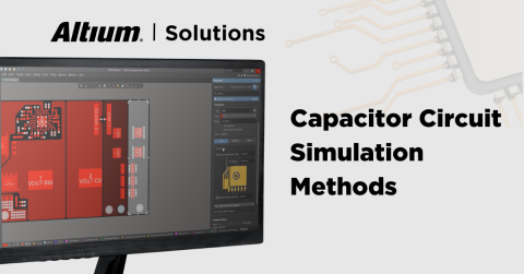
The Best Capacitor Circuit Simulator for PCB Design
A capacitor is a fundamental element in integrated circuits and in PCB design, and it’s hard to think of a circuit that doesn’t contain at least one capacitor. A capacitor’s behavior and interaction with other components in a circuit generally needs to be simulated to ensure the design will operate as intended. Capacitors can provide filtering, blocking, and power stability behavior depending on their use in a circuit, and a capacitor circuit
Read Article
Pagination
First page
« First
Previous page
‹ Previous
…
Page
143
Page
144
Page
145
Page
146
Current page
147
Page
148
Page
149
Page
150
Page
151
…
Page
160
Page
170
Page
180
Page
190
Page
200
Page
210
Page
220
Page
230
Page
240
Page
250
Page
350
Next page
Next ›
Last page
Last »
Subscribe to