How Vibration and Electric Shock Affect Your PCB

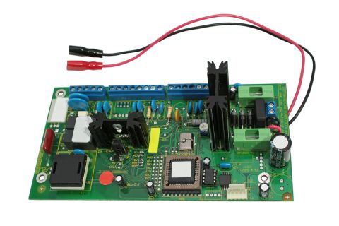
There are many mechanisms that can cause a PCB to fail, but some common failures can be traced back to vibration and electric shock. Vibration and electric shock are estimated to account for approximately 20% of PCB failures as they affect the most sensitive portions of a PCBA: the components.
With the best set of PCB design tools, a designer can implement some basic design decisions that will help ensure reliability and prevent failure due to vibration and electric shock. Things like correct stackup design, component selection, and overvoltage protection design will help prevent failure and can be easily implemented with Altium Designer. Here’s how Altium Designer helps you protect your circuit board assembly from failure.
ALTIUM DESIGNER
A unified PCB design application with advanced layout features for professional use.
Electric shock, vibration, mechanical shock, and thermal runaway are four major causes of failure in PCBs. Among these four causes, two of these are estimated to cause 20% of all failures in PCBs, yet they are quite easy to prevent if you have the right set of design tools. The fact these two failure modes are so common has led to many industry standards governing electronics design, both at the component level and PCB level.
Designing a board to have a low chance of failure due to mechanical vibration and electrostatic discharge requires some simple component selection priorities and design choices. Altium Designer gives you the supply chain features you need to find components for your circuit board that can withstand electric shock. You can also implement some basic layout decisions that help prevent electrostatic discharge from harming your components should it occur.
Prevent Failure from Electric Shock
Electrical shock in a PCB occurs due to electrostatic discharge whenever there is a large potential difference between two charged conductors. When the electric field between two charged conductors is large enough, the dielectric separating the conductors can break down into a plasma, allowing current to flow between the two conductors. At minimum, this creates a small corona discharge, while in the worst case it can lead to ignition and destruction of the board.
Simple methods to implement discharge protection in your PCB focus on layout between high and low voltage sides of the board, and on component selection. These include:
- Use of surge suppression components, like TVS diodes or gas discharge tubes
- Isolation between low and high voltage circuitry with transformers and optocouplers
The best PCB layout tools with supply chain visibility can help you succeed in both areas, giving you everything needed to
Use Altium’s Design Rules and Components for Electric Shock Protection
The rules-driven design engine in Altium Designer lets you implement industry standards on creepage and clearance in your PCB to help protect sensitive circuitry from ESD and failure. You can define industry standards like IPC 2221, IEC 62368-1, and application-specific industry standards as design rules to help you stay compliant with safety requirements. You can also find the components you need for surge suppression and circuit protection as you work through your design, and all without using a separate program for finding components.
- Creepage and clearance are two important requirements in the IPC 2221 and IEC 62368-1 standards.
Learn more about high voltage PCB design standards on creepage and clearance.
- A TVS diode is a popular method for suppressing electric shock and voltage surges in an electronic circuit.
- You can find the ESD protection components you need with the Manufacturer Part Search Panel in Altium Designer. You’ll have a comprehensive view of the electronics supply chain.
Learn more about using the Manufacturer Part Search Panel in Altium Designer.

The Manufacturer Part Search Panel in Altium Designer
Ensure Reliability Against Mechanical Vibration
Mechanical vibration can cause a board to fail in two ways:
- Vibration fatigue can occur in solder joints, particularly at the top sides of solder balls and fillets on SMD components
- The board itself can bend and flex, leading to solder and component lead damage within the bending region
Even small amounts of vibration over a long period of time will cause vibration fatigue and failure in component leads and soldered connections. Protecting soldered connections requires suppressing vibration with secure mechanical fixing to the enclosure and adding damping at the fixation point. Nyloc nuts will friction lock the board on its standoffs and can help keep the board with friction damping.
Design Your Enclosure and Mounting Strategy to Prevent Vibration Failure
The CAD tools in Altium Designer allow mounting components like nuts and screws to be added to a PCB layout, just like any other component. Mounting holes are also easy to design, and templates can be created to place multiple mounting holes on large assemblies. Altium Designer’s MCAD utilities also allow the entire board, including mounting components, to be viewed in 3D to ensure a tight fit to the enclosure.
- Any mounting style in a circuit board needs to be implemented while preventing interference between components and mechanical mounts.
- Working in 3D MCAD tools requires STEP models for all components to ensure accurate placement and enclosure design.
Learn more about using STEP models in your PCB design software.
- The MCAD engine in Altium Designer allows electrical and mechanical co-design in a single application, including enclosure design in popular MCAD applications like SolidWorks.
Learn more about Altium Designer’s ECAD/MCAD collaboration features.

Design your mechanical mounting style to prevent vibration in Altium Designer.
Rules-Driven Design Tools Help You Create Reliable PCB Layouts
Altium Designer is the ideal tool software package for electronics design and layout as it includes all the required design utilities in a single application. Everything needed for reliable PCB design and layout is included in Altium Designer. The power of Altium Designer lies in its rules-driven design environment, which allows you to access every design tool you need in one application. While other design platforms separate your important design tools into different programs, Altium Designer keeps you productive and helps you design the most reliable circuit boards.
Design the Most Reliable Circuit Boards in Altium Designer
The rules-driven PCB design engine in Altium Designer is built for productivity and reliability. Important design rules for protecting against electric shock and vibration can be checked as the PCB layout is created, helping you spot errors before manufacturing. Once you’re ready for production, your manufacturing tools will generate project documentation without the need for an external program.
- Stay productive and ensure quality when you use Altium Designer, the only PCB design platform with a complete set of design tools for any application.
Learn more about Altium Designer’s unified design environment.
- Altium Designer’s ECAD/MCAD engine is accessible alongside industry-standard PCB layout and routing tools to help you stay productive and design high-quality products.
Learn more about the native ECAD/MCAD design engine in Altium Designer.
- When you’ve finished your design and you’re ready to share with your manufacturer, you can use the Altium 365 platform to release and review your project data for safety and reliability.
Learn more about sharing your PCB project data through the Altium 365 platform.

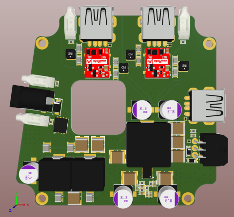
3D view of an LED PCB in Altium Designer.
Protecting your circuit board design from vibration and electric shock is much easier when you use Altium Designer’s rules-driven design engine. No other design application provides a complete set of design, sharing, and design verification features in a single application.
Altium Designer on Altium 365 delivers unprecedented integration to the electronics industry until now relegated to the world of software development, allowing designers to work from home and reach unprecedented levels of efficiency.
We have only scratched the surface of what is possible to do with Altium Designer on Altium 365. You can check the product page for a more in-depth feature description or one of the On-Demand Webinars.


