


What is the High-Speed Signal Frequency Range and Bandwidth?

At a Glance
The high speed signal frequency range and bandwidth will affect signal integrity. Use the best design tools that can accommodate broadband signals in your PCB.


Go back to your university math classes and recall the Fourier spectra; this concept tells you that digital signals can be represented as an infinite sum of frequencies, with the representation normally beginning at the clock frequency. From here, definitions of signal bandwidth start to get very muddy, with many arbitrary definitions being applied to define frequency limits on a digital signal.
In reality, a digital signal is not a perfect square wave and can only be approximated by the Fourier frequency of a perfect square wave. Additionally, much of what is done in high-speed PCB design involves designing a channel bandwidth to accommodate a certain signal bandwidth, even though many supposed experts on high-speed PCB design do not actually know that they are doing this.
To clarify these points, my objective in this guide is to explain what the bandwidth of a digital signal is and how designers should focus on channel bandwidth instead of being preoccupied with signal bandwidth.
Channel Bandwidth Versus Signal Bandwidth
When we talk about the frequency range of a high-speed signal, the important parameter is the power concentrated at different frequencies. In theory, the high-speed signal frequency range extends out to infinity, but your PCB design software needs to use some upper limit to determine the appropriate bandwidth of a high-speed digital signal. There are several ways to define the frequency range:
- Using the knee frequency, or about 35% of the inverse of the rise time
- In terms of the signal’s 5th fundamental harmonic
- As the receiver’s Nyquist frequency
The correct answer is “none of the above.”
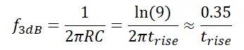
In a recent poll on LinkedIn, one of my connections asked the community what is the bandwidth of a digital signal. Invariably, almost every person who responded referred to the knee frequency, which is defined as follows.
The knee frequency is an incorrect measure of high-speed signal frequency range
This formula is an incorrect value for digital signal bandwidth because it has nothing to do with signal bandwidth that is sourced from a high speed driver. The knee frequency is a measure of bandwidth in an RC circuit before low-pass filtering action occurs, where the 10% - 90% rise time is defined by the RC time constant. This RC time constant can be considerably different than the signal sourced from a high-speed driver.
Because knee frequency is based on a measurement of rise time for a capacitive circuit, it is, in actuality, a channel bandwidth. It only applies when the channel is infinitely short. Real channels in a high-speed PCB may not behave this way. The faster the buffer circuit is in the digital driver, the less likely knee frequency will be valid.
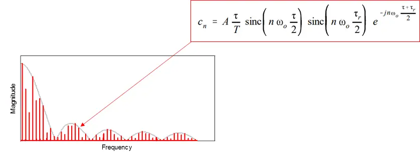
In reality, digital signals have infinite bandwidth even when they have a finite rise time. The power spectrum of a digital signal is given by a set of harmonics with a sinc function amplitude envelope, with periodic dropouts being a function of the rise time and repetition rate.
Harmonics in a digital signal with a sinc function envelope defining the amplitude. Note that this causes some harmonics to have zero power.
No matter what, the digital driver in a high-speed channel will always try to source a signal with infinite bandwidth. However, the channel that carries the signal to the receiver will create losses that limit the bandwidth. Your job in high-speed PCB design and RF PCB design is to design channels (i.e., transmission lines) that provide some minimum amount of bandwidth so that enough signal can pass to the receiver, and the receiver can then recover useful information from the signal.
What Limits Channel Bandwidth?
There is one thing that limits channel bandwidth: losses. All loss mechanisms in a high-frequency channel serve to limit the bandwidth of the signal when the signal reaches the receiver. So, in a PCB, what are these loss mechanisms which the designer can attempt to control? These are return loss, insertion loss, and mode conversion (for differential pairs). Any loss mechanism falling into these two categories can limit the ability of the channel to transfer power to a receiver.
In PCB design, all channels will limit signal bandwidth; it is just a matter of the extent to which a signal's bandwidth becomes limited due to the channel bandwidth. Beyond just knowing the types of loss and various loss mechanisms, it is important to know the various elements in a PCB that contribute to these losses.
|
Signal bandwidth |
|
|
Channel bandwidth |
Limiting factors in channel bandwidth
|
To quantify bandwidth, we have some tools available which will assist in determining which loss mechanisms are excessive; this involves the use of S-parameter simulations and measurements. Whenever the S-parameter results indicate that there is a bandwidth limitation (through high return loss, insertion loss, and mode conversion), it is the designer’s job to find the bandwidth-limiting elements in the channel and modify the design.
Fixing Channels With Limited Bandwidth (Too Much Loss)
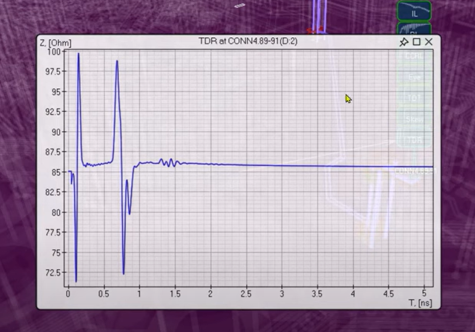
From the perspective of bandwidth limiting due to excessive losses, fixing a channel with limited bandwidth requires determining whether the channel losses are reflection-dominated or insertion loss-dominated. This can be determined from a time domain reflectometry (TDR) measurement.
When the TDR measurement shows significant reflection, then these should be minimized if it is determined that the return loss is excessive within the channel bandwidth requirement. An example from our recent Altium OnTrack podcast interview with Yuriy Shlepnev is shown below; watch the full episode here.
Simulated TDR measurement from Simbeor.
Based on the time coordinate in the TDR plot, it’s possible to determine the impedance discontinuity at each point along a trace and modify the channel as required to ensure minimal reflection. In other instances, where there is little reflection but excessive loss, a lower loss material or shorter route may be needed.
In the case of differential pairs, the third possible form of loss, mode conversion, can be determined from a mixed-mode S-parameter plot. This will show conversion of differential power to common-mode power, which would then be suppressed by the differential receiver. To learn more, read our guide on mode conversion in differential pairs.
Whether you need to build reliable power electronics or advanced digital systems, use the complete set of PCB design features and world-class CAD tools in Altium Designer®. To implement collaboration in today’s cross-disciplinary environment, innovative companies are using the Altium 365™ platform to easily share design data and put projects into manufacturing.
We have only scratched the surface of what’s possible with Altium Designer on Altium 365. Start your free trial of Altium Designer + Altium 365 today.

About Author
Related Resources
Related Technical Documentation
Table of Contents
Design to Release, Without the Friction
- Keep reviews tied to the right version
- Reduce handoff confusion and rework
- Spot sourcing and release risk earlier
- Work solo, share when needed
Get Started
Thank you, you are now subscribed to updates.

