


3D-MID in Focus: Principles, Processes, and Practical Use


Due to the miniaturization of electronic components and improvements in manufacturing and assembly processes, design trends are increasingly moving toward smaller, high-performance devices. For example, smartwatches and smart glasses now integrate powerful processors, displays, cameras, microphones, speakers, Bluetooth, Wi Fi, and built in antennas, among other features.
This evolution challenges designers to continually reduce the space occupied by the electronics. One solution is 3D-MID technology, which allows for the integration of mechanical and electronic components. Altium, a leader in design tools, offers a unique solution in the market for three-dimensional circuit design.
What is 3D-MID?
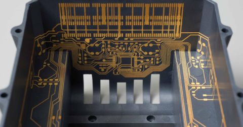
The acronym 3D-MID stands for 3-Dimensional Mechatronic Integrated Devices. It refers to a technology that integrates electronics directly into a mechanical component, using the part’s own material as the substrate. This approach enables the formation of conductive traces and the addition of component pads directly on the plastic as demonstrated in the following example figure:

Figure 1: 3D-MID Example
In other words, it creates a PCB where the substrate is the same material as the mechanical part (such as ABS or Polycarbonate), saving space by eliminating the need for a separate PCB and its assembly. This method not only conserves space but also allows designers to adapt circuits to complex geometries—whether curved or angular—thereby overcoming the limitations of traditional methods. Even with flexible PCBs, it is crucial to consider torsion angles, create proper routing pathways within the mechanical structure, and secure mounting points to prevent undesired movement that could lead to damage.
The manufacturing process behind this technology is called Laser Direct Structuring (LDS). This patented process by LPKF involves injection molding a thermoplastic material doped with a non conductive metal compound. A laser then activates this compound to form the PCB traces. Additionally, 3D printing can serve as an alternative to injection molding, broadening the accessibility of this technology.
This technology can also be combined with techniques such as Wire Bonding.
History, Present, and Future of 3D-MID
The LDS technique was developed in the late 1990s through a collaboration between Technische Hochschule Ostwestfalen Lippe (THOWL), the University of Applied Sciences in Lemgo, Germany, and LPKF. Exploitation rights were held by LPKF until 2022, when all patents were transferred to the company.
Although 3D-MID is not new and has been applied in various fields, its impact on the industry is growing—especially with companies like HARTING actively promoting its use across diverse industrial sectors. The evolution of Electronic Design Automation (EDA) tools, such as those from Altium, further enhances its accessibility to PCB designers.
Looking ahead, the future of 3D-MID technology is promising. While current LDS processes support only a single copper layer (albeit with complex geometries), advancements may soon enable multilayer designs. Such progress would allow for high-speed buses with controlled impedance to be integrated into signal layers. Furthermore, 3D printers are increasingly playing a critical role in advancing both the technology and its applications.
What are the Applications of 3D-MID?
3D-MID technology offers extensive application versatility across various sectors, including:
- Automotive: Used in sensors for climate control systems, switches, mechanically integrated antennas, LED lighting, and Adaptive Cruise Control (ACC).

Figure 2: Devices used in automotive sector
- Antenna Integration: Integrating antennas directly into the mechanical design adapts them to the component’s geometry. This innovation not only saves space but also enables three dimensional design—an important advantage at high frequencies. In RFID, antennas can be mounted directly within the housing along with the chip, eliminating the need for a separate PCB and reducing production costs.

Figure 3: Antennas example
- Medical Devices: Miniaturization and weight reduction enabled by 3D-MID allow for the creation of innovative devices, such as hearing aids that integrate electronics into the casing. This results in less invasive treatments and novel drug delivery systems.

Figure 4: Hearing aid based on 3D-MID technology
- Industrial Applications: From drones to RFID tags and payment terminals, 3D-MID optimizes space and weight while streamlining manufacturing processes. In security applications, it enhances tamper detection and physical protection.

Figure 5: Safety caps for payment terminals
Manufacturers like HARTING have even developed specialized component carriers and PCB expanders to support these applications.

Figure 6: HARTING’s 3D-MID Usage Example
And… What is the Design Process Using 3D-MID Technology?
This section briefly outlines the steps for creating a basic design using Altium Designer 25:
- Component Selection: Start by designing or selecting the 3D component where the electrical part will be integrated. Note that design rules must be followed to ensure proper trace routing and component placement (considering factors like curvature radii and flat mounting areas). For example, an ABS enclosure from Hammond Manufacturing may be used; in this case, the bottom cover might house a connector, an LED, and a resistor.

Figure 7: ABS Enclosure from Hammond Manufacturing
- Project Creation: Create a new project in Altium, add a schematic, and edit it. The schematic for this example is kept simple.

Figure 8: Schematic Design in Altium Designer 25
- PCB Document: Next, create a new PCB document, selecting the PCB3D option. Altium will prompt you to select a 3D component (in STEP or IGES format). In this example, the enclosure is selected from the manufacturer’s website, and Altium loads it as the new substrate.

Figure 9: New PCB 3D

Figure 10: Selected 3D Model
- Design Transfer: Transfer the design to the PCB as you would with any conventional design. Components are loaded onto the PCB file as with a standard PCB.

Figure 11: PCB Update from Schematic Design

Figure 12: Loaded components from schematics
- Component Placement and Routing: Position the components on the surface and trace the lines accordingly.

Figure 13: Component Placement

Figure 14: Routing
- Export: Once the design is complete, export the 3D-MID design data via File » Export » 3D MID. The exported data includes the substrate and copper pattern as a STEP assembly (required for the LDS process) along with a 3D pick and place file.
What are the Manufacturing and Assembly Processes?
The manufacturing process, known as Laser Direct Structuring (LDS), involves several key steps:

Figure 15: Laser Direct Structuring Process
- Injection Molding: A one component injection molding process uses approved thermoplastic material with additives. Although this method can be expensive for low volume production, 3D printing offers a cost effective alternative.
- Laser Activation and Structuring: A laser beam activates the non conductive metallic particles in the thermoplastic material to form the circuit traces.
- Metallization: An electroless process applies a nickel layer followed by a thin gold layer.
- Assembly: Standard Surface Mount Technology (SMT) processes are used for component placement and solder reflow.
What are the Limitations of This Technology?
Despite its advantages, 3D-MID technology has several limitations:
- The additive material used as a substrate can only be activated by a laser on its surface—and only once. This means the technology currently supports only single-layer designs (except for external layers activated on both sides).
- This restriction limits its application for routing high-speed signals that require embedded differential pairs or controlled impedance between specific ground planes.
- Other design limitations include minimum trace thickness, spacing between conductors, via types, surface finish options, availability of power planes, challenges with high-density component boards, and issues with very small packages such as BGAs or WLCSPs.
Conclusions
3D-MID: A Solution for New Challenges
In today’s rapidly evolving landscape, where devices are becoming increasingly compact, the emergence of innovative technologies is essential. 3D-MID technology empowers designers to create circuits directly on the surface of three-dimensional parts, conforming to complex geometries. This not only saves space but also reduces production costs by eliminating separate PCB assembly processes.
Altium Designer as a 3D-MID Design Tool
Altium Designer 25 stands out as an ideal tool for 3D-MID design, integrating seamlessly into the standard electronics design workflow. By leveraging pre existing libraries and traditional design processes, designers can synchronize schematics with 3D models, place components directly on the 3D surface, and route them using conventional tools. Manufacturers like HARTING recommend Altium Designer as a preferred tool for 3D MID applications.
Design and Manufacturing Limitations
It is important to acknowledge that 3D-MID technology has inherent design and manufacturing limitations. Designers must use manufacturer approved materials, avoid overly complex electrical designs, and steer clear of multilayer stack-ups, non through hole vias, and high speed lines that require precise impedance control. Additionally, mechanical constraints, particularly regarding laser activation and component positioning, must be carefully considered.
Learn more
- Altium's 3D Circuit Technology (in cooperation with HARTING)
- Altium 3D‑MID Feature Page
- Altium Documentation: 3D‑MID Design
- HARTING 3D‑MID Examples of Automotive Applications
- HARTING 3D‑MID Examples of Medical Applications
- HARTING 3D‑MID Examples of Industrial Applications
- Research Association Mechatronic Integrated Devices
- Authorized LDS Manufacturers
- PCB Expander – Design Freedom in Limited Space
- 3D‑MID Component Carrier – Intelligent Connections

About Author
Related Resources
Table of Contents
Design to Release, Without the Friction
- Keep reviews tied to the right version
- Reduce handoff confusion and rework
- Spot sourcing and release risk earlier
- Work solo, share when needed
Get Started
Thank you, you are now subscribed to updates.

