


How Structural Electronics Is Reshaping Electrical Engineering

At a Glance
Explore how structural electronics merges form and function, enabling lighter, smarter designs that redefine the future of electrical engineering.


In today’s rapidly advancing field of electrical engineering, structural electronics are redefining the status quo.
Rather than isolating circuitry within protective housings, structural electronics embed electronic functionality into the very materials that support and shape a device.

This shift marks a foundational change in how engineers design, fabricate, and apply electronic systems.
How Structural Electronics Breaks Down Traditional Boundaries
For decades, electronic design followed a rigid model: engineers mounted electrical components onto circuit boards and enclosed them within protective housings. This method drew a hard line between functional electronics and the structures that supported them. Structural electronics erase that line by embedding circuits, sensors, and active components directly into the structural materials.
This level of integration unlocks new possibilities. Devices shed unnecessary weight by removing redundant enclosures. Designs gain flexibility, no longer limited by the need to accommodate standalone circuit boards. Most significantly, functionality expands, and electronics can now distribute across the entire structure, not just in isolated modules.
Key Technologies Driving the Structural Electronics Revolution
Structural electronics have shifted from experimental to practical due to advancements in several interlocking technologies. Breakthroughs in flexible conductive materials, additive manufacturing, lightweight composite structures, and printed electronics have made it possible to embed functionality directly into structural elements without compromising durability or performance. Together, these innovations redefine what’s possible in modern product design, enabling electronics to disappear into the form factor while still delivering high performance.
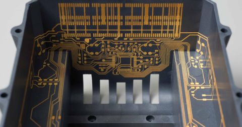
3D-MIDs (3-Dimensional Mechatronic Integrated Devices)
3D-MIDs represent one of the most promising approaches to structural electronics. These devices are essentially plastic molded substrates with traces running along any surface, including at right angles and running vertically. The manufacturing process, known as Laser Direct Structuring (LDS), uses a laser to etch the circuit pattern directly onto the surface of a 3D substrate, which then undergoes metalization treatment to build up conductive pathways.
HARTING, the industry's leading supplier of MID products, has developed innovative component carrier MID substrates that act as vertical adapters for devices with standard footprints. These carriers allow designers to vertically mount an SMD part with a standard footprint, and the carrier is soldered to the board just like any other SMD component.

Printed Electronics
Printed electronics uses conductive, resistive, and dielectric inks to create circuits directly on or within structural materials. Unlike traditional PCB manufacturing, which is a reductive process (etching away copper from a continuous sheet), printed electronics is an additive process where signal pathways are printed directly onto a substrate.
When a design requires pathways to cross over each other, a small patch of dielectric material is printed in that location, sufficiently expanded beyond the crossover to achieve the required level of isolation between different signals. This approach eliminates the need for multiple layers separated by dielectric materials, as in traditional PCBs.
Flexible and Stretchable Electronics
The development of flexible substrates and stretchable conductive inks has liberated electronics from the rigidity of traditional PCBs. These materials can bend, twist, and stretch while maintaining electrical functionality, making them ideal for integration into dynamic structural components.
Specialized materials can achieve 100-1000% elongation while maintaining conductivity, typically through geometric designs (serpentine or fractal patterns), composite materials (conductive particles in elastic matrices), or liquid metal alloys in elastomeric channels.
In-Mold Electronics (IME)
IME technology allows electronic circuits to be printed onto a flat film, which is then thermoformed and injection molded, creating a three-dimensional part with embedded electronics. This process eliminates assembly steps, reduces weight, and creates more durable products by protecting electronic components within the structure itself.
Structural Electronics Industry Applications Transforming Engineering Practice
Structural electronics are already transforming design and production strategies across a variety of sectors. Their influence extends beyond the lab, driving new approaches to product architecture in commercial and industrial settings. By combining mechanical structure with electrical function, these systems simplify form factors, reduce component counts, and unlock new levels of efficiency.
Engineers now apply structural electronics to solve real challenges in industries that demand innovation under strict performance constraints. Let's examine how this technology is shaping advancements in automotive engineering, aerospace and defense, consumer electronics, and medical devices.
Automotive Engineering
Modern vehicles are increasingly incorporating structural electronics into their design. Touch-sensitive control surfaces are being integrated directly into dashboards and door panels, eliminating the need for separate buttons and switches. Heating elements are being embedded into structural components rather than added as separate systems. And sensors for everything from occupant detection to structural health monitoring are being built directly into the vehicle's frame and body panels.
Tesla has pioneered the integration of electronics into structural components. Their vehicles feature center console touch panels with haptic feedback created using in-mold electronics, steering column controls printed directly onto 3D surfaces, and door panels with integrated lighting, controls, and electronic functions. The result is a 30% reduction in dashboard assembly complexity, 15% weight reduction, and higher reliability due to the elimination of mechanical buttons and connections.
Aerospace and Defense
Weight reduction is a critical concern in aerospace applications, making structural electronics particularly valuable. Aircraft manufacturers are exploring ways to integrate antennas directly into wing structures, embed health monitoring systems into critical components, and create multifunctional materials that can serve both structural and electronic purposes simultaneously.
Airbus has implemented structural electronics in several aircraft systems, including lightning strike protection integrated with wing structure electronics, fuselage panels with embedded strain gauges for structural health monitoring, and embedded antenna systems that eliminate aerodynamic drag. Their A350 XWB incorporates over 1,000 sensors embedded in structural components, reducing weight by 200kg compared to conventional approaches while providing significantly enhanced monitoring capabilities.
Consumer Electronics
Perhaps the most visible application of structural electronics is in consumer devices. Through IME, TactoTek, a lead company in this domain is revolutionizing product design through innovative headphone solutions. Modern headphones utilizing structural electronics integrate components directly into curved structural elements, allowing designers to optimize physical curvature for intuitive interaction while maintaining a sleek aesthetic with transparent materials and subtle metallic finishes. These designs incorporate LED indicators embedded within the structure to communicate device status, touch-sensitive controls without separate button assemblies, and curved form factors that would be challenging to achieve using conventional manufacturing—all while reducing weight and improving durability. This approach represents a significant departure from traditional electronics, which would require separate circuit boards and mechanical assemblies, resulting in bulkier products with more potential failure points.
Medical Devices
The medical field is benefiting from structural electronics through the development of conformable diagnostic equipment, smart prosthetics with embedded sensing and actuation, and implantable devices that can better match the contours of the human body.
Ultra-thin conformal sensors that adhere directly to the skin, integrated accelerometers, ECG, and EMG in a single flexible substrate, and stretchable circuits that move naturally with the body are revolutionizing patient monitoring. Clinical studies have shown these systems provide medical-grade data quality while being significantly more comfortable for patients than traditional monitoring equipment, increasing compliance rates by over 60%.
Electrical Engineering Challenges and Solutions
The promise of structural electronics introduces a new set of engineering problems that demand interdisciplinary solutions. Embedding active components into materials that also serve structural functions complicates everything from thermal dissipation to electrical isolation and long-term durability. Engineers must rethink traditional design workflows to accommodate electrical performance and mechanical stability in tandem. Innovations in conductive materials, advanced simulation tools, and co-design platforms now provide a foundation for solving these challenges and turning structural electronics into a reliable, scalable design strategy.
Thermal Management
When electronic components are embedded within structural materials, traditional cooling approaches like heat sinks and fans may be impossible to implement. Engineers are developing innovative solutions including phase-change materials, micro-fluidic cooling channels integrated into the structure, and thermally conductive structural materials.
Reliability and Maintenance
Traditional electronics can be repaired by replacing discrete components or entire circuit boards. Structural electronics presents challenges for maintenance and repair, as electronic functions are integrated into the structure itself. This is driving the development of self-healing materials and modular approaches that allow for targeted replacement of failed sections.
Design Methodologies
Structural electronics requires engineers to think differently about design. Rather than designing the electronics and structure separately, they must be considered as a unified system from the earliest stages. This is driving the development of new CAD tools that can simultaneously model mechanical, thermal, and electrical properties, as well as advances in multi-physics simulation.
Altium: Leading the Structural Electronics Revolution
Altium has positioned itself at the forefront of structural electronics design with capabilities that extend beyond traditional PCB design. Its unified design environment enables engineers to manage complex electrical layouts across unconventional substrates and embedded architectures. By supporting multi-board systems, rigid-flex configurations, and advanced 3D modeling, Altium allows designers to simulate and validate electronics that operate as part of the physical structure. With real-time collaboration through Altium 365 and seamless ECAD-MCAD integration, engineers can refine functional and mechanical aspects simultaneously. These tools make it possible to implement distributed sensors, embedded interconnects, and shape-conforming circuits directly within a product’s structure, setting the stage for a new generation of intelligent, integrated devices.
3D Electronics Design
Altium's 3D PCB design capabilities allow engineers to visualize and design electronic circuits that conform to non-planar surfaces and integrate with mechanical structures. The new 3D-MID tool brings true 3D circuit design to Altium for the first time, allowing you to combine electrical and mechanical functionality into a single part.

A 3D-MID document integrates into your Altium project in the same way as a standard PCB - its components and connectivity are driven by your schematic design, and it incorporates standard SMT footprints from your usual component library.
MCAD-ECAD Co-Design
Native integration with mechanical CAD systems enables seamless collaboration between electrical and mechanical engineers, essential for structural electronics design. When designing the substrate in MCAD, 3D curves can be placed on the surface of the part and included in the exported IGES file. These "curves" can then be displayed in Altium and used as a guide for placing components and regions, and during routing.
Printed Electronics Support
Altium also supports printed electronics design, where the circuit is printed directly onto a substrate. The layer stack can be configured for printed electronics, with conductive and non-conductive layers defined according to the manufacturing process. Dielectric shapes can be manually created or automatically generated to isolate crossovers between different nets.
Manufacturing Output
Altium can generate the manufacturing data required for production of structural electronics. For 3D-MIDs, the design can be exported in formats compatible with Laser Direct Structuring (LDS) machines. For printed electronics, outputs include files for each conductive printing pass and each dielectric printing pass, typically in Gerber format.
Structural Electronics and the Evolving Role of Electrical Engineers
As structural electronics advances, electrical engineers will shift from designing discrete circuit boards to architecting systems where form and function converge within the product’s structure.
Interdisciplinary Collaboration
The line between electrical engineering and other disciplines like mechanical, materials, and chemical engineering will continue to blur. Successful implementation of structural electronics requires expertise across these domains, driving more collaborative approaches to design and development.
New Educational Paradigms
Engineering education will need to evolve to prepare students for this interdisciplinary future. Curricula that have traditionally separated electrical and mechanical engineering will need to create crossover courses that teach integrated design principles.
Evolving Standards and Practices
Industry standards and best practices will need to adapt to this new paradigm. From design validation to testing methodologies to end-of-life considerations, the structural electronics revolution will necessitate a rethinking of established norms.
Redefining Systems Through Structural Electronics
Structural electronics marks a shift in both technology and mindset, dissolving the long-held division between structural integrity and electronic functionality. By embedding intelligence into the very materials that shape a product, engineers can now achieve levels of efficiency, performance, and integration that were previously out of reach.
As the field progresses, electrical engineers stand at the threshold of a profound evolution—one that allows them to architect systems where mechanical form and electrical behavior coalesce. Platforms like Altium make this transformation actionable, equipping engineers with the tools to prototype, simulate, and realize these complex designs within a unified environment.
While the transition away from traditional board-based thinking may seem daunting, those who adopt this model early will lead a new era of design innovation.
Explore how Altium supports printed electronics and enables the integration of electrical circuits with three-dimensional mechanical parts.

About Author
Related Resources
Table of Contents
- Breaking Down Traditional Boundaries
- Key Technologies Driving the Revolution
- 3D-MIDs (3-Dimensional Mechatronic Integrated Devices)
- Printed Electronics
- Flexible and Stretchable Electronics
- In-Mold Electronics (IME)
- Industry Applications Transforming Engineering Practice
- Automotive Engineering
- Aerospace and Defense
- Consumer Electronics
- Medical Devices
- Engineering Challenges and Solutions
- Thermal Management
- Reliability and Maintenance
- Design Methodologies
- Altium: Leading the Structural Electronics Revolution
- 3D Electronics Design
- MCAD-ECAD Co-Design
- Printed Electronics Support
- Manufacturing Output
- The Future of Electrical Engineering
- Interdisciplinary Collaboration
- New Educational Paradigms
- Evolving Standards and Practices
- Conclusion
Design to Release, Without the Friction
- Keep reviews tied to the right version
- Reduce handoff confusion and rework
- Spot sourcing and release risk earlier
- Work solo, share when needed
Get Started
Thank you, you are now subscribed to updates.