PCB Design Rules Related to SAP

Change. Trying something new? Are these things that you are comfortable with and excitedly embrace, or is the unknown something that makes you nervous and skeptical? Personally, I can firmly answer, “that depends.” I do like to try new things, most of the time. Please don’t ask me to jump out of an airplane – but I am all in for travel adventures and new experiences.
For those that have followed my blogs for a while, you also know that I excitedly embrace new printed circuit board technologies. Flex, rigid-flex, complex HDI constructions, and new materials, all make me excited to be working in a dynamic, ever-changing industry. I enjoy being on the leading edge and helping engineers and printed circuit board designers navigate the learning curve of technology advances.
“The more things change, the more they stay the same” ~ Alphonse Karr
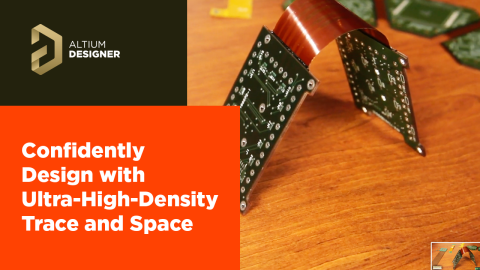
Recently, this blog series has been diving into SAP, semi-additive PCB processes. These processes are now commercially available for low to medium volume, high mix applications and are giving PCB designers another tool in their toolbox. The ability to now route with a 25 micron, or even a 12.5-micron trace, and space is exciting.
We have gone through the basics of SAP processing and recently looked at some of the top questions related to the printed circuit board stack up.
Now, let’s dig a little deeper into the printed circuit design rules. I am going to start with the fact that there are not many firm design rules specifically relating to SAP processes at this time, at least when reviewing through the lens of a low to medium volume fabricator. The high-volume commercial market does have some pretty stringent design rules that must be followed.
Does that make designing with these ultra-high-density feature sizes a little uncomfortable? If you are nodding your head while reading this, count yourself in the majority. There are a lot of questions and a decent learning curve to navigate. The good news is that there are a lot of people working on this and data and experience are being gathered at a rapid pace.
Let me start by stating that there are many more things that DO NOT change when looking at PCB design using these ultra-high-density feature sizes. We are all familiar with the “design rules” or fabrication guidelines that our fabricators publish. These are typically long lists of printed circuit board design parameters giving minimum or maximum guidelines and are often broken into segments, something along the lines of standard, advanced and emerging PCB fabrication capabilities. We are all also comfortable with the knowledge that each fabricator has their own slightly different capabilities and preferences. I don’t expect this to change as PCB fabricators add SAP processing to their capabilities.
What else will not change? What can we be comfortable with?
The semi-additive PCB process specially addresses how to form traces on a circuit layer and shifts the fabrication limitation from an etching constraint, which is typically at about 75 microns (.003”) to a photolithography limitation. Most fabricators that have purchased laser direct imaging equipment in the past few years have the capability to resolve circuit trace and space to 25 micron and a few have the ability to resolve to 12.5 micron. Most processes not related to the process of forming the traces in each layer remain unchanged.
Hole size and via formation capabilities. The minimum hole size for mechanical drilling and laser drilling will remain the same as will the fabricators’ ability to manufacture blind and buried vias, staggered or stacked microvias. Plating tolerances, aspect ratio capabilities and plated or non-plated hole to edge tolerancing also remains the same.
Solder mask is another capability that does not change with SAP. The materials, tolerances, and capabilities for via tenting, via fill, materials and colors don’t need to change when looking at SAP processes.
Surface finishes also remain the same. ENIG, ENEPIG, Silver, OSP, whatever finishes your fabricator offers will be compatible with SAP layers. This comes with one caveat. Hot Air Solder Level is not recommended if outer layers are manufactured with SAP layers.
What are some of the things that will change?
The most significant change is circuit trace width and spacing, in multiple aspects. First, the feature sizes can now be shrunk to 25 micron or below. (Check with your fabricator for their specific capabilities.) This is exciting when looking at how to navigate complex BGA routing. Not only can finer feature sizes be used, but the tolerance on those traces will be much tighter than with subtractive etch processes, significantly impacting controlled impedance tolerances. The sidewalls of those circuit traces are now going to be straight sidewalls rather than the trapezoid we typically model with.
These three things have a significant impact on routing, layer reduction, and overall design simplification. They also have a significant impact on signal integrity. The benefits are easy to identify and yet they come with challenges to the way that we typically think of PCB design. As we continue through this blog series, we will tackle some of these opportunities for learning how to apply these ultra-high density feature sizes to printed circuit board design. As always, please reach out with specific questions at any time!
About Author
Related Resources


Related Technical Documentation
Take advantage of the world's
most trusted PCB design system.
One interface. One data
model. Endless possibilities.
Effortlessly collaborate with
mechanical designers.
The world's most trusted
PCB design platform
Best in class interactive
routing
View License Options
Thank you, you are now subscribed to updates.