


Cost Comparison: Subtractive vs. Semi-Additive

At a Glance
Expert Tara Dunn discusses the significant benefit of the 3D additive manufacturing process in space savings associated with routing at 15 or 25 microns compared to the standard 75 microns. Read now and learn more about cost comparison with the subtractive process.


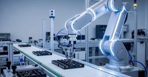
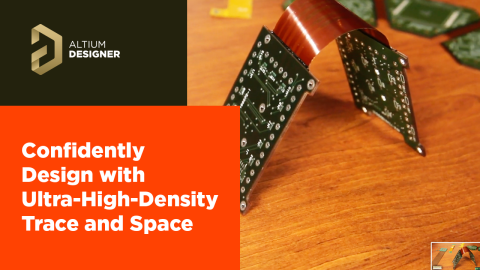
I am very enthusiastic about the semi-additive processes now available to PCB fabricators of all sizes and spend a fair amount of time talking about potential designs that could benefit from the ability to route with 15 micron or 25-micron trace and space. While mSAP has been utilized in select very high-volume manufacturing facilities in Asia, for technology such as smart phones, it is a technology that has largely been unavailable for low to medium and even what most consider high volume PCB applications. With the launch of the A-SAP™ process (Averatek’s Semi-Additive Process) this technology is now available by a number of printed circuit board fabricators which opens this up to all PCB designers to use in a wide spectrum of applications.
While I much prefer discussing printed circuit board design guidelines and connecting designers with fabricators skilled in this technology and can meet their fabrication requirements, the question of cost invariably filters into the discussion. So let’s address that elephant in the room today.
First, for those unfamiliar with the semi-additive PCB process, please refer to a few of our previous blogs. We have gone through the basics to SAP processing, and recently looked at some of the top questions related to the printed circuit board stack up, explored some of the “design rules” or “design guidelines” that do not change when designing with these ultra-high-density feature sizes. and explored the design space around the possibility of utilizing these ultra-high density circuit trace widths in the BGA escape regions and wider traces in the routing field. The benefit is a reduction in circuit layers and the concern is maintaining 50-ohm impedance. Eric Bogatin recently published a white paper analyzing just this benefit and concern.
What is the comparative cost of this technology when comparing against subtractive processes, same layer count, trace geometries, via count etc.?
This is a common question and one that I will answer with the same reasoning that I have often used when talking about flexible circuit technology compared to rigid printed circuit board technology. All things being equal, including layer count, circuit trace and space, hole and pad size, volume, etc., a flexible circuit is going to be more expensive. Fabricating flexible circuits and rigid flex technology takes a special skill set, special handling, and the flexible materials themselves are more expensive than standard rigid materials. If you do not have a driving need to use flexible materials, don’t.
But today’s electronics designs push the limits and there are many benefits to moving to flexible materials and often the added cost is inconsequential in the bigger picture of the overall design.
The same is true with the A-SAP™ process. If you were going to compare a 6-layer PCB design on standard FR4, 3 mil line and space, 8 mil drill to that same design built with an additive PCB fabrication process rather than a substrative PCB process, it would simply be more expensive. The additive process requires a specialized process and process control. Comparing SAP to subtractive etch in this way does not address the benefits and even the overall cost savings that could be realized when routing with these ultra-high density circuit board features.
What is another way to look at the cost of this technology and the benefits of a 15 micron or 25-micron line and space?
For the discussion today, we won’t dive into the signal integrity benefits of the semi-additive process. Instead, we lets look at the other significant benefit, the space savings associated with routing at 15 or 25 microns compared to the standard 75 microns. This space savings is key when talking about a cost comparison. Let me share a few examples:
- A design with subtractive etch requires 12 layers and 3 lamination cycles. This design is redesigned reducing the layer count to 8 and the lamination cycles to 1. Keeping in mind that added lamination cycles typically result in an approximate 40% increase in cost. The reduction in complexity in this design increases yield and reduces cost, even when calculating the increased cost of SAP. That is a win for the PCB design.
- What if you don’t use that space for added routing and use it for increased hole and pad size? An 8-layer design with micro vias top and bottom could be redesigned to through hole technology. Again, a cost savings to the overall design.
- What if the driving need for your design is miniaturization and the routing space saved is utilized to reduce the overall size of the printed circuit board? Even with the same technology and layer count, if more parts are up on the PCB production panel, the overall cost of the design could decrease.
As you can see, it is really a disservice to try to make an apples-to-apples comparison between cost for a subtractive etch technology and a semi-additive technology. The real gains are when this new fabrication process is used to reimagine the PCB design and simplify complexity.
As a parting thought ~ the A-SAP™ process is also applicable to larger feature sizes. For those of you with a particularly troublesome design that may not yield well with 75 micron or 65-micron traces with subtractive etch, changing the technology from subtractive to additive is likely to increase the yield and deliver a more reliable product.
About Author
Related Resources
Design to Release, Without the Friction
- Keep reviews tied to the right version
- Reduce handoff confusion and rework
- Spot sourcing and release risk earlier
- Work solo, share when needed
Get Started
Thank you, you are now subscribed to updates.

