


PCB Design: What are Aspect Ratios and Why Are They Important?

Any via in a PCB can cause reliability problems, which relate to the size of the via and the materials used in the PCB. When a via is placed in a PCB, the drill size and the depth into the PCB define a via's aspect ratio. It is this parameter that is an important determinant of via reliability. The ability to reliably fabricate vias with different aspect ratios depends on several factors. For example, some manufacturers will quote you very high aspect ratio vias which they can fabricate and prove reliability in accelerated stress testing.
The via aspect ratio you use in your PCB depends on the drill size you can reliably fabricate to the board. There are some practical constraints and rules of thumb to consider when designing your vias to have a target aspect ratio. I will examine some of these points in this article, both for mechanically drilled vias and microvias.
What is Via Aspect Ratio in PCB Design?
The aspect ratio of a via in a PCB has a very simple mathematical definition. The via aspect ratio is the ratio of the drill depth to the drill diameter used to manufacture the via:
AR = (Drill depth)/(Drill diameter)
For standard thickness PCBs, where the thickness is 62 mils or 1.57 mm, the maximum aspect ratio you could expect to see for mechanically drilled through-hole vias is 10:1. This is because the smallest drill diameter typically used for PCB fabrication is 6 mils, and this value with the standard thickness gives the maximum 10:1 ratio. Due to tool consumption in 6 mil diameter drills being faster than with larger drills, the higher cost of 6 mil vias is overcome by using a larger drill diameter, which gives a smaller aspect ratio.
I will typically use 10 mil diameter drills at the low end unless a BGA footprint or high-pin density connector footprint demands I use a smaller drill diameter. In other words, I could expect a maximum 6:1 aspect ratio in most PCBs I design.
PCB Via Aspect Ratio and Reliability
Now that we have defined typical aspect ratio values, how does a via's aspect ratio affect its reliability?
This is an important question as it partly relates to differences in reliability between mechanically drilled holes and laser-drilled holes used in HDI PCBs. As rules of thumb, primarily to ensure reliability of the drilled plated structures, the typical limits on the aspect ratios are as follows:
- Through-hole vias: 12:1 or smaller
- Laser-drilled blind/buried vias: 1:1 or smaller
Of course, these are just rules of thumb, and all rules of thumb are made to be broken. The case of an approximately 12:1 through-hole via with a 7 mil drill would only be typical in a 2 mm thick board. Cases where you start to see through-hole vias with very high aspect ratios tend to be in non-standard PCBs that have larger thicknesses, and in such a case, consultation with your fabricator regarding the allowed drill size for through-holes is necessary.
That being said, I recall taking a tour with Summit Interconnect in 2021, and their process engineering manager stated that they could reliably fabricate high aspect ratio vias with 6 mil drills and prove their reliability. The expertise of the fabricator and their ability to prove reliability is quite important here and it underscores the need to contact them early, particularly when your board is non-standard.
Another factor that is not often considered is the plating thickness in the via hole. Typically, this could be approximately 1 mil, but of course, you could ask your fabricator to over-plate it. Via walls with thicker copper will be more reliable, so it should not be surprising that you could expect higher aspect ratio allowances when the plating is thicker.
The same applies when using blind and buried vias, whether laser-drilled or mechanically drilled. In fact, for laser-drilled vias, particularly those that will be stacked, lower aspect ratios become more common at higher layer counts, primarily because the dielectric thickness gets smaller.
Laser-Drilled Microvias and Larger PCB Aspect Ratios
Microvias can also have larger aspect ratios depending on the size of the drilled hole and the quality of the copper wrap plating in sequential lamination. For through-hole vias, IPC reliability standards also specify via aspect ratios ranging between 6:1 and 8:1. A via aspect ratio of 8:1 is considered to be something of a required capability among PCB manufacturers.: According to IPC-T-50M, laser drilled microvia should have a maximum aspect ratio of 1:1.
This could arise in a few possible ways:
- The use of skip vias to span two or more layers
- The use of a thicker dielectric in the HDI buildup layers
- Novel processes that deposit small diameter vias in thicker layers
Stacking of microvias is not necessarily the same as using a single high aspect ratio via. The reliability in a stack will depend on the aspect ratio of an individual via and the number of vias in the stack. These days, HDI fabricators have the expertise to build ELIC layer stackups, which will stack blind/buried microvias throughout the PCB stack-up. If you have a high layer count PCB with fine pitch BGAs, and you opt to go the stacked microvia route, make sure you contact your fabricator and determine the appropriate aspect ratio for the microvias in the stack to ensure reliability.
PCB Via Plating Challenges
Drilling vias will require some understanding of the intricacies that involve adding depth into your circuit and adding fabrication necessities. The PCB via aspect ratio affects the difficulty with which the interior can be plated. Copper is deposited on the interior of a via using plating solution. The plating solution must be able to wick into a via hole by capillary action in order to fully plate the interior of the via.
The physics and chemistry involved in micropillar plating are very interesting. During capillary action, surface tension draws the plating solution into the via, and copper begins depositing along the wall. Due to the meniscus that forms at the surface of the solution, the copper precursor is consumed quickly from the solution in deeper regions of the via. As a result, the inner portions of a via barrel can have thinner plating than at the edges of the via.
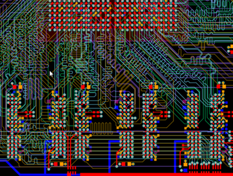
![]()
Small diameter vias on an HDI board
If the PCB via aspect ratio is larger, then there is a risk that the deposited copper in the via wall will be thinner, and the center of such a via would be more prone to cracking under thermal stress. This could be solved by adjusting the viscosity of the plating solution, but more practically the approach for compensating this effect is to set the appropriate throwing strength in the electroplating process for a high aspect ratio via. This not only improves the structural strength of the via but also improves its reliability against thermal stress.
Whether you need to build reliable power electronics or advanced digital systems, use the complete set of PCB design features and world-class CAD tools in Altium. To implement collaboration in today’s cross-disciplinary environment, innovative companies are using Altium to easily share design data and put projects into manufacturing.

About Author
Related Resources
Related Technical Documentation
Table of Contents
Altium is transforming the electronics industry so thoroughly that our web pages need a minute to catch up. For a short time, some information on this page may be outdated.
We appreciate your patience. It will be worth the wait!
Learn More
Thank you, you are now subscribed to updates.