


Explain Like I’m a Designer: ELIC PCB and HDI Routing

At a Glance
Using ELIC in your HDI PCB can help you maximize your connection and component density. Read more about using ELIC for high density interconnect routing.


Under the IPC-2226 standards, there are several standard PCB stackups used to support HDI PCB rouitng, which then allows trace routing into fine-pitch BGA components. Most of the standard HDI PCB stackup constructions use a core (buried) via, and/or a through-hole via touching all layers. Standard HDI PCB stackups might also use skip vias on the surface layer in addition to standard blind/buried microvias in order to allow BGA breakouts to access the inner layers of a PCB.
With PCBs containing even more layers and becoming thinner than ever before, new techniques are used to increase interconnect density. The most complex HDI routing and stackup design style in use today is called every layer interconnect (ELIC). This routing style follows a simple idea: extend microvias throughout the entire PCB stackup so that signals can route on high density interconnects between any set of layers in the PCB. This might sound like an innocuous allowance, but it places constraints on the manufacturing process and material sets used to build the PCB. We'll look more at ELIC in this article.
Designing an ELIC PCB Stackup
ELIC is sometimes referred to as any-layer HDI, meaning signals can be routed on high density interconnects between any layer in the stackup. These advanced HDI PCBs contain multiple layers of copper-filled stacked in-pad microvias that enable even more complex interconnections. When using ELIC on an HDI board, each layer has its own copper-filled, laser-drilled microvias. ELIC uses only stacked copper-filled microvias to make connections through each layer. This allows connections to be made between any two layers in the PCB once the layers are stacked. Not only does this offer an increased level of flexibility, but it also allows designers to maximize interconnect density on any layer.
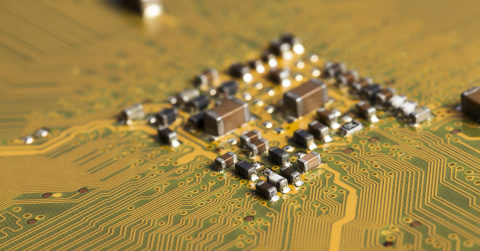
The image below shows a side cross-sectional view of an ELIC HDI stackup. This microsection image contains stacked microvias throughout the PCB stackup, but it could also contain staggered microvias in different regions.

Through-hole vias are not needed anymore since all connections between the board are fabricated in the initial buildup. Since ELIC uses a copper-filled structure, plating techniques for filled vias (e.g., VIPPO) are not required. This particular stackup goes against the IPC warning on microvia reliability as we have stacked microvias spanning across the entire PCB stackup. Not all fabricators that can guarantee yield for ELIC PCBs without latent defects from reflow. Be careful when selecting a manufacturer that can provide these guarantees and be sure to implement their DFM rules to ensure your board will pass quality and acceptance criteria.
ELIC Manufacturing
The ELIC manufacturing process starts with an ultra-thin core with laser-drilled microvias and a solid copper-filled base. After the initial microvia on an inner layer is filled with copper, the next dielectric layer is added in sequential lamination. Laser drilling is applied to the new layer to build the ELIC PCB stacked, followed by filling the vias in that layer with copper. This is repeated until the desired stack is built with copper-filled microvias. The sequential copper fill improves the structural integrity of the board and is needed to prevent dimpling/voiding in the interior microvias as long as buildup produces strong plating interfaces should stacked microvias be used.
DFM for ELIC PCBs
In general, there are a few simple DFM rules that should be followed when floorplanning an HDI PCB that will use ELIC. In addition to following the recommendations of your HDI fabrication house, make sure you implement these general recommendations:
- Choose the appropriate microvia aspect ratio to ensure reliability in the fabricated bare board
- Make sure to specify filled microvias in the internal layers to prevent voiding/dimpling
- Carefully pair up layer thickness with clearance and trace width for impedance controlled lines to ensure you can execute your fanout strategy
- The layer arrangement must be made symmetric throughout the device
ELIC Applications
ELIC has found a home in PCBs used for GPUs and memory cards, but newer smartphones, tablets, and wearable devices can also be designed using ELIC. These applications tend to require components with high pin count and fine pitch. These boards also tend to use 10 or more layers. Using ELIC in these applications allows designers to route the required interconnects in boards with a small footprint.
ELIC PCB stackups are commonly used in high-speed applications that require high IO density, such as in FPGAs where multiple interfaces are being instantiated in the device. ELIC may also be used in some boards that must support RF routing on PTFE materials. In either case, impedance mismatch and resulting return loss will dominate in these lines as routes can typically be short. It's possible to route across layers without leaving stubs in these boards as backdrilling will not be needed. However, as routes get longer, dielectric losses on these routes will start to dominate and will limit the useful trace length. Keep these points in mind when selecting materials for your HDI board.
ELIC has also become common some HDI rigid-flex PCBs. Package sizes have been reduced even further by combining ELIC-capable PCBs with folded rigid-flex boards in a single package as long as any bend region is chosen to prevent excess stress on microvia stacks. The standard design techniques for flex ribbons apply as they would in other applications, but the use of ELIC allows ribbons to be integrated into smaller PCBs.

Inner signal layers in high density, high speed designs will have multiple ground/power planes that can help shield signal layers from each other and reduce crosstalk. This aids EMC compliance by shielding excess radiation. There are some moderate layer count stackups that can support high density fanouts and aid EMC compliance; creative layout strategies in these boards can help keep signal layer counts low and allows the use of additional ground, which has the dual effect of reducing crosstalk and EMI.
When you're ready to build up your ELIC PCB stackup for your advanced design, use the layer stack design and routing features in Altium Designer® to build your board. The built-in CAD tools and the ActiveRoute® feature make HDI routing using ELIC a breeze. When you’re ready to release these files to your manufacturer, the Altium 365™ platform makes it easy to collaborate and share your projects.
We have only scratched the surface of what’s possible with Altium Designer on Altium 365. Start your free trial of Altium Designer + Altium 365 today.

About Author
Related Resources
Related Technical Documentation
Table of Contents
Design to Release, Without the Friction
- Keep reviews tied to the right version
- Reduce handoff confusion and rework
- Spot sourcing and release risk earlier
- Work solo, share when needed
Get Started
Thank you, you are now subscribed to updates.

