


Mastering Blind and Buried Vias in HDI PCBs

At a Glance
View our complete list of resources on usage of blind and buried vias in HDI PCB design.


The next time you decide to use a BGA package in your PCB, it might require laser-drilled blind and buried vias. A new designer may find blind and buried vias usage to be complex, but never fear a little complexity. We compiled essential resources you'll need to use blind and buried vias successfully in an HDI PCB.
Blind and buried vias are not new technology; they have been around since the advent of integrated circuit substrates used in many semiconductor packages. Blind/buried vias do require following some important design rules related to the reliability of the structure. The resources compiled below will address these manufacturing aspects of blind and buried vias so that designers can be successful.
Starting Out with Blind and Buried Vias in HDI PCBs
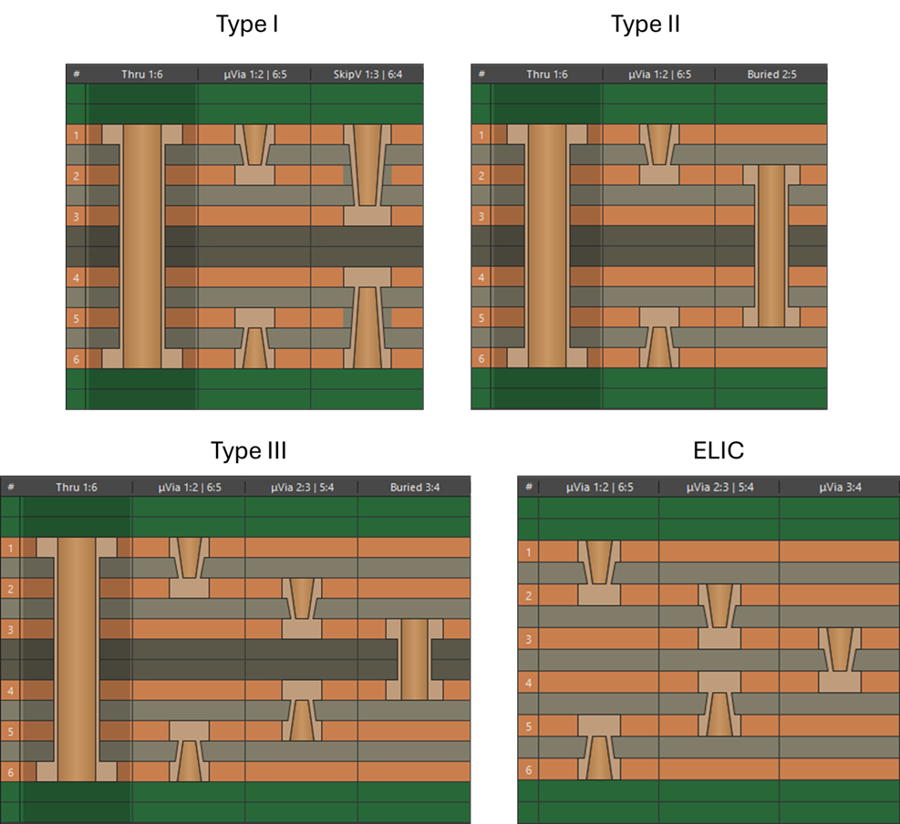
Blind vias and buried vias are two of the standard interconnects used in HDI PCBs for vertical routing. Through-hole vias and skip vias are also used, depending on the stack-up and fabrication process for an HDI PCB. This selection and arrangement of vias in an HDI PCB lead to the standard stack-up constructions shown below.
From here, you can already see the layer assignments in HDI PCB stack-ups involving blind, buried, core, through-hole, and in some cases, skip vias. The manufacturing process used to produce these stackups leverages plating processes that allow vias to be stacked, as well as starting and stopping on the same layer; this is not possible with mechanically drilled blind/buried vias.
The buildup process for a Type II or Type III HDI stackup is shown below; the same process is essentially used with Type I stackups, but with an extra drill step on the outer buildup film lamination. The process below is shown for a standard 2+N+2 HDI stackup, where the core via is buried in the thick central region of the PCB stackup, and the buildup film layers are laminated above and below. With each blind via spanning a single layer, a large number of stacked/staggered microvias could be required to fanout a very large fine-pitch BGA.
Match the HDI Stack-Up to a BGA Package
Blind vias and buried vias are normally selected based on the need to route into/out of a particular package, normally a BGA. They are selected when mechanically drilled through-hole vias will require excessively large diameters and will not fit beneath a BGA package without violating copper-to-copper clearances or when the number of sub-laminations with mechanically-drilled blind/buried vias becomes too large.
For example, in the STM32 BGA footprint presented in the video below, you have the option to use through-hole vias or blind and buried vias for the fanout routing. If blind and buried vias are used, the layer count can be kept lower, and this may make compliance with etch tolerances simpler. However, if etch tolerances allow, you could use larger through-hole vias when the stack-up already has a high layer count.
Sizing Your Blind and Buried Vias
Once you determine that blind and buried vias are the best option for fanout routing and you've determined the appropriate stack-up, you will need to size the hole diameter and pad size for the blind and buried vias.
The hole and pad sizes used for blind and buried vias are selected based on the thickness of the dielectric layer. The goal is to maintain a small aspect ratio (ratio of hole diameter to thickness). You will also need to select the hole diameter based on the process used to place the vias in the circuit board:
- Mechanical drilling can be used down to 6 mils and can be used for any PCB dielectric.
- Laser drilling can be used below 6 mils and can be used only on specific dielectrics.
Ideally, keep the aspect ratio below 2 for individual blind and buried vias, and ideally keep the aspect ratio at 1 or less if you will stack blind and buried vias up to high layer counts (3 or more layers). Unless you are building an exotic design, you may be required to stagger your blind and buried vias at some point. Make sure to check the stack-up and via assignments with your HDI fabrication house to ensure the board can be produced successfully.
Which Dielectric Should Be Used?
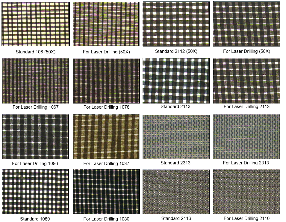
When laser-drilled microvias are required in your design, then laser-drillable prepregs will be needed for the outer build-up layers of the HDI stack-up. Laser-drillable prepregs come in many varieties and resin formulations, and they are built with many possible glass weave styles. These material types are discussed by Happy Holden in this linked article.
The article I have linked above contains the following image prepared by Happy. This image shows the possible glass weave styles used in standard prepregs and laser-drillable prepregs used for HDI layer stack-ups.
Based on these available materials and the via size you are targeting for fanout routing, you can then find a commercially available dielectric material for the HDI build-up layers that has an acceptable thickness value. The thickness can be chosen based on the aspect ratio range you want to hit for your blind and buried vias. That essentially completes your layer stack-up for an HDI PCB, and the only step remaining will be to design transmission lines for any high-speed interfaces.
Summary
Blind and buried vias are a big enabler of many advanced products, but the selection of blind and buried vias revolves around other important engineering decisions. Aspects such as ball or pad pitch in component packages and the overall layer count needed in the design are some of the factors that will drive the sizing of blind and buried vias. If blind and buried vias are needed, you can consider the following process for sizing them and pairing them with a layer thickness:
- Estimate the layer count based on pin counts in BGAs or high-density connectors.
- Select a standard HDI stack-up and layer thicknesses.
- Based on the most dense pad or ball pitch, determine the pad and hole size needed for blind and buried vias.
- Based on the hole diameter, determine if laser drilling is needed and select a compatible material that hits the thickness target.
This completes the process for aligning your blind and buried via sizes with the materials in your stack-up while ensuring reliability.
Finally, make sure you determine whether mechanically drilled vias with multiple laminations or laser-drilled microvias with sequential lamination will produce the required fanout routing without excessive plating on the surface layers. When the number of mechanically drilled blinds becomes large, it might cost less and lead to a simpler design when microvias and build-up layers are used.
Whether you need to build reliable power electronics or advanced digital systems, use the complete set of PCB design features and world-class CAD tools in Altium Designer®. To implement collaboration in today’s cross-disciplinary environment, innovative companies are using the Altium 365™ platform to easily share design data and put projects into manufacturing.
We have only scratched the surface of what’s possible with Altium Designer on Altium 365. Start your free trial of Altium Designer + Altium 365 today.
About Author
Related Resources
Related Technical Documentation
Table of Contents
Design to Release, Without the Friction
- Keep reviews tied to the right version
- Reduce handoff confusion and rework
- Spot sourcing and release risk earlier
- Work solo, share when needed
Get Started
Thank you, you are now subscribed to updates.