Why Use Plated Through Hole Technology in PCB Design?

When it comes to technology, we never look back. Sometimes, it seems that the old technology just won't phase out. One example can be seen in plated through hole mounting technology for your electronic components; this class of legacy components seems to hang around to this day, even as new designs require ever smaller components.
But is it really that simple? Why use through-hole technology in printed circuit boards (PCBs) when it seems surface mount technology (SMT) components are smaller and allow more compact component placement in your PCB? Like most design decisions, there are tradeoffs involved using each type of component. To start, let’s give a quick breakdown of plated through hole mounting technology and surface mount technology as it pertains to the printed circuit board PCB design process.
What are Through-Hole Components?
Just like all other components, plated through hole circuit board components can be roughly divided into active and passive components. Each type of component mounts to the board in the same way. The designer needs to place through-holes in their PCB layout, where the hols are surrounded with a pad on the surface layer for soldering. The through-hole mounting process is simple: place the component leads into the holes and solder the exposed lead to the pad. Plated through hole circuit board components are large and rugged enough that they can be easily hand soldered. For passive through-hole components, the component leads can be quite long, so they are often clipped to a shorter length before mounting.
Passive Through-Hole Technology
Passive through-hole components come in two possible types of packages: radial and axial. An axial through-hole component has its electrical leads running along the component's axis of symmetry. Think about a basic resistor; the electrical leads run along the cylindrical axis of the resistor. Diodes, inductors, and many capacitors are mounted in the same way. Not all through-hole components come in cylindrical packages; some components, like high power resistors, come in rectangular packages with a lead wire running down the length of the package.
Side view of an axial through-hole mounting component.
Meanwhile, radial components have electrical leads that protrude from one end of the component. Many large electrolytic capacitors are packaged in this way, allowing them to be mounted to a board by running the lead through a hole pad while taking up a smaller amount of space on the circuit board. Other components like switches, LEDs, small relays, and fuses come packaged as radial through-hole components.
Radial (left) and axial (right) electrolytic capacitors.
Active Through-hole Components
If you remember back to your electronics classes, you'll likely remember the integrated circuits you used with dual-inline package (DIP) or plastic DIP (PDIP). These components are normally seen as being mounted on breadboards for proof-of-concept development, but they are commonly used in real PCBs. The DIP package is common for active through-hole components, such as op-amp packages, low-power voltage regulators, and many other common components. Other components like transistors, higher power voltage regulators, quartz resonators, higher power LEDs, and many others may come in a zig-zag in-line package (ZIP) or transistor outline (TO) package. Just like axial or radial passive through-hole technology, these other packages mount to a PCB in the same way.
Through-hole components came about at a time when designers were more concerned with making electronic systems mechanically stable and were less concerned about aesthetics and signal integrity. There was less of a focus on reducing space taken up by components, and signal integrity problems were not a concern. Later, as power consumption, signal integrity, and board space requirements began to take center stage, designers needed to use components that provide the same electrical functionality in a smaller package. This is where surface-mount components come in.
Surface Mount Technology
If you take a look at any modern PCB design, you’ll likely see boards that are dominated by surface mount components. Newer designs still use through-hole components, but these components tend to be used more often in power electronics and other devices that generate a lot of heat. Surface mount technology is the most commonly used component package technology today. These types of components do not use pins for electrical leads. Instead, the leads appear as small pads of metal on the same side of the component. The primary purpose of these pads is to allow soldering directly onto the surface of a PCB during assembly.
The use of pads in surface mount technology compared to through hole technology provides certain advantages, which will be discussed below. In addition, the smaller pad size and overall component size causes these components to have less prominent parasitics. This allows them to be operated at higher speeds/frequencies before you start to notice signal integrity problems.
If you remember your old PC, you probably remember Pentium processors with the array of pins on the bottom of the package. This type of package is called a pin grid array (PGA), which is similar to the more modern land grid array (LGA) package. A PGA component may look like a through-hole component, but it does not solder into holes on the board. Instead, it plugs into a surface-mounted package that solders onto the board. This allows the PGA component to be easily replaced or upgraded if needed.
Through-hole vs. Surface Mount Costs
Surface mount components tend to be smaller than an equivalent through-hole component. However, this does not necessarily mean the cost of a surface mount component is always cheaper simply because less raw materials are used in manufacturing these components. Surface mount components themselves might cost a similar price as an equivalent through-hole component. However, once automated assembly costs per component are considered, the total cost per surface mount component tends to be cheaper than a through-hole component with the same component values, power/voltage ratings, and tolerances.
This difference arises because placing through-hole components requires drilling holes in your PCB, which incurs tooling costs. In contrast, drilling is not required with surface mount components, which accounts for the cost difference. All this begs the question: if surface mount components are smaller, faster, and cheaper, then why use through-hole mounting technology at all? The answer depends on the use case for your PCB design. Yes, through-hole PCB technology is old, big, and expensive, but there are some advantages.
Through-hole Technology: Advantages and Disadvantages
|
PRO |
CON |
|
Easier for prototyping |
Higher board cost due to drilling |
|
Strong physical connections |
Takes up more board real-estate |
|
Heat tolerance |
PCB assembly process is more involved |
|
Power handling capability |
Slower speeds |
Surface Mount Technology: Advantages and Disadvantages
|
PRO |
CON |
|
Small size → Denser boards |
Weaker physical connections to the PCB |
|
Reduced parasitics → reliable at higher speeds |
Lower heat tolerance |
|
Faster & cheaper assembly |
Lower power handling capability |
|
No drilling → Cheaper board fabrication |
DFM: tombstone, pop cornering, etc |
When comparing the two PCB design technologies, it's easy to see why surface mount is the reigning champ. Surface mount components are smaller, cheaper, and can be run at higher speeds. This is especially important in upcoming mixed signal and analog-heavy applications like IoT devices, new wireless devices, and wearables. As network speeds increase and new devices run at higher data rates, surface mount components will continue to make an appearance as they generally cannot be substituted for through-hole components.
The issue with parasitics in through-hole components and the parasitics created in the PCB layout creates a challenge for automotive, aerospace, and military products that need to be very rugged yet also need to operate far into GHz bands. There are many challenges where a through-hole component can create greater insertion loss along an interconnect at mmWave frequencies. However, through-hole components are desired in these applications as the solder points are less likely to fail during operation. There is still plenty of innovation that can occur in this area.
Technology leaders are also driving towards a connected society, and size does matter when it comes to PCB design. In the drive for ubiquitous computing, IoT, or the “ambient intelligence” we all crave, the drive to make smaller and smaller components includes the board itself. Smaller components enable smaller boards, allowing us to build printed circuit boards in almost any form factor. Smaller sizes mean lower manufacturing costs. Less expensive components and boards provide cost savings to the end customer.
Through-hole mounting technology is great for prototyping and testing as you’re able to easily swap out components on a printed circuit board. Even before you design your board, you can breadboard your design with through-hole technology.
In addition to prototyping and testing, through-hole components have very strong physical bonds to the board as they are soldered from both the top and bottom of the board. This makes boards with through-hole mounting technology very durable, which is partly why they are used in military and aerospace. They also have a high temperature tolerance. You can find through-hole technology in all sorts of places. One example is on LED lights in billboards or stadiums. Through-hole LEDs are extremely bright and durable, allowing them to handle the outside elements.
Also, if you look at industrial machines and equipment, you can find many boards that are built almost exclusively using through-hole components. Again, this is due to the harsh operating conditions, such as extremes of temperature or situations involving high power consumption. Through-hole technology may be old and seem outdated, but it has a purpose and can be used for its physical endurance and strength in today’s connected world.
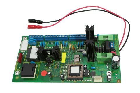
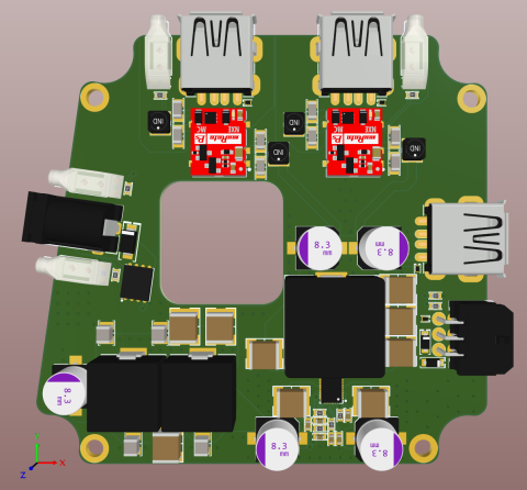
Through-hole components in a power supply
Altium Designer on Altium 365 delivers an unprecedented amount of integration to the electronics industry until now relegated to the world of software development, allowing designers to work from home and reach unprecedented levels of efficiency.
We have only scratched the surface of what is possible to do with Altium Designer on Altium 365. You can check the product page for a more in-depth feature description or one of the On-Demand Webinars.
Curious to learn more? Visit our popular PCB design guidelines blog and learn from our experts.

