


Flex Circuit Coverlay: Design with Lamination Processes In Mind


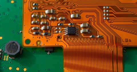
Flex circuit coverlay is a laminated polyimide film and adhesive system used to protect copper circuitry in flexible PCBs. Unlike photoimageable soldermask, coverlay shifts during lamination and adhesive flows under heat and pressure, making registration, aperture sizing, and geometry critical factors in flex circuit manufacturability and long-term reliability.
For those new to flexible circuit design, this is a common scenario: the layout looks great, pads are centered in their openings, and clearances meet the design rule specification. And then the first article comes back.
Under magnification, a few pads showed slight adhesive creep along the edge. There is nothing too noteworthy, but it is enough that the assembler noticed inconsistent wetting on a fine-pitch component near the bend area. Neither the design nor the stack-up changed. The difference? The way coverlay with adhesive behaves differently from the way soldermask does.
In CAD, coverlay can feel like soldermask. It still functions as a protective layer with defined openings. But in fabrication, coverlay is a laminated polyimide film with adhesive that is placed, aligned, pressed, heated, and cured. It moves during that process, and adhesive flows when heated. That mechanical behavior is so important to understand and accommodate in flex circuit designs.
Key Takeaways
- Coverlay behaves fundamentally differently from soldermask. Although coverlay appears similar to soldermask in CAD, it is a laminated polyimide film with adhesive that shifts and flows during heat and pressure processes. Designers must account for this mechanical behavior early.
- Adhesive flow and registration directly affect pad reliability. During lamination, adhesive flows and redistributes, which can reduce pad exposure, especially in fine‑pitch areas. Proper aperture sizing, rounded openings, and realistic tolerances are critical.
- Geometry choices impact long-term flex durability. Sharp corners, slits, and poorly placed seams can introduce stress concentration points that lead to cracking or fatigue. Design openings with smooth shapes and avoid critical features in bend zones.
- Flex and rigid-flex require system-level thinking. Material movement, thermal cycles, and adhesive behavior compound across lamination steps. Designers must treat the board as one integrated mechanical system, not separate rigid and flex domains.
Why Flex Circuit Coverlay Behaves Differently Than Soldermask
On a rigid board, soldermask is typically photoimageable, which means it is applied, exposed, developed, and cured in place. Once cured, lateral movement is minimal, and the photoimaging process holds a tight tolerance.
While soldermask more or less stays where you put it, coverlay responds to mechanical forces. Alignment depends on tooling pins and on material stability, and adhesive behavior depends on copper distribution and local geometry. All of this collectively means that pad exposure can and often will end up slightly different than the CAD image, and this material shift and adhesive squeeze-out can be addressed at the design stage.
Adhesive Flow: The Part People Forget About
During lamination, adhesive seeks the path of least resistance. In areas with tight apertures or heavy copper, the flow pattern changes. If openings are sized too tightly to the pad outline, adhesive can encroach just enough to reduce effective pad exposure.
Sharp internal corners in coverlay openings are another risk. Adhesive tends to pool slightly at corners during flow. Over time, those corners can also become stress concentration points during flexing.
From the fabrication side, a few design adjustments consistently improve outcomes:
- Increase coverlay openings beyond the copper pad outline with realistic clearance.
- Favor rounded or teardrop-style apertures rather than sharp internal corners.
- Avoid assuming one-to-one copper-to-coverlay registration capability in fine-pitch zones without confirming fab tolerances.
Understanding how laminated adhesive behaves under heat is key to achieving reliable flex circuit performance and consistent assembly results.
Registration
Rigid materials are dimensionally stable, while flexible materials expand more readily with heat. During lamination, polyimide shifts slightly, and adhesive shrinks slightly after cure. Tooling pins constrain movement, but never perfectly.
Individually, those movements are small and often unnoticeable, but with a fine-pitch connector region, small can become meaningful.
Designers sometimes specify very tight coverlay clearance around pads to maximize solderable area. From a lamination standpoint, that leaves little margin for natural material movement.
If you are designing for fine pitch in flex:
- Confirm realistic coverlay registration capability with your fabricator.
- Build in exposure margins to account for normal variation in flex PCB manufacturing processes.
- Consider copper balancing in high-density zones to reduce uneven adhesive thickness.
Corners, Slits, and Bend Zones
Flex circuits bend, which seems obvious. What’s less obvious is how coverlay geometry affects long-term durability.
Sharp internal corners in openings act like tiny crack initiators. Slits introduced for relief can propagate under repeated flexing if placed in dynamic bend areas. Even subtle differences in coverlay thickness across a bend zone influence stress distribution.
From a fabrication and reliability perspective:
- Round internal aperture corners wherever possible.
- Keep coverlay seams and relief cuts outside dynamic bend zones.
- Coordinate bend radius with total material stack thickness, including adhesive.
Stiffeners Change Everything
Stiffeners add another layer of complexity. Acrylic and epoxy adhesives behave differently during lamination. The different expansion rates between the stiffener and flex core can introduce localized stress.
Near stiffener transitions, you can see:
- Slight adhesive squeeze-out.
- Minor coplanarity variation.
- Increased stress concentration during flex.
From a design standpoint:
- Clearly define stiffener material and adhesive systems.
- Allow adequate clearance for adhesive flow.
- Avoid stacking multiple thickness transitions in tight, high-stress areas.
Assemblers feel these effects quickly: Connectors may sit inconsistently, and solder joints near stiffener edges may experience higher stress during handling.
Rigid-Flex Adds Cumulative Movement
In rigid-flex constructions, coverlay may be applied before or after rigid lamination, depending on the stack-up strategy. Each lamination cycle introduces thermal movement and adhesive behavior. Sequential lamination compounds these dimensional shifts. Resin flow in rigid sections influences adjacent flex zones and the registration tolerances stack.
Designers sometimes treat rigid and flexible areas as separate domains. Fabrication treats them as one integrated thermal process. That distinction is important when you’re defining stackups.
If possible, bring your fabricator into the stack-up discussion before footprint rules are frozen. Lean into their experience.
Looking at First Articles Differently
When reviewing first articles, it helps to look beyond pad exposure symmetry. Ask:
- Is adhesive evenly distributed around apertures?
- Do corners show stress whitening or micro-cracking?
- Is pad exposure sufficient for assembly margin, not just theoretical alignment?
Coverlay is not a static coating. It becomes part of a dynamic mechanical system that must survive bending, temperature cycling, and assembly heat.
Flex technology gives designers extraordinary packaging freedom: Folding, bending, wrapping. These are interconnect strategies that rigid boards simply cannot achieve.
In CAD, coverlay is a layer. In fabrication, it is a laminated film under pressure and heat. In the field, it becomes a structural element in motion. Understanding that shift in perspective changes how you design openings, define tolerances, and review first articles.
Designing Flex Circuits with Greater Confidence Using Altium Develop
Flex circuit performance is determined long before fabrication, during stackup planning, coverlay definition, and layout decisions that must account for lamination behavior. Altium Develop helps engineers keep these design details visible and connected as the design evolves, so material behavior, geometry choices, and manufacturability constraints are considered early, when changes are still low‑cost.
By keeping schematic intent, layout decisions, and supporting data aligned in one place, Altium Develop reduces the need for manual reconciliation and helps designers move from design to review to release with fewer surprises, especially in complex flex and rigid‑flex applications.
Learn more about Altium Develop and get started →
Frequently Asked Questions About Flex Circuit Coverlay
What is the difference between coverlay and soldermask in flex PCB design?
Coverlay is a laminated polyimide film bonded with adhesive, while soldermask is typically photoimageable and fixed in place. Unlike soldermask, coverlay can shift during lamination and adhesive can flow, which means designers must allow for movement and avoid tight, rigid assumptions about pad exposure.
Why does adhesive flow cause problems in flex circuits?
During lamination, adhesive flows under heat and pressure, especially around tight apertures or high copper density areas. This can reduce effective pad exposure or create uneven coverage, leading to poor solder wetting or assembly variability if not accounted for in the design.
How should I size coverlay openings for reliable assembly?
Coverlay openings should be larger than the copper pad outline, with added clearance to account for material movement and adhesive flow. Designers should also use rounded or teardrop apertures instead of sharp corners to prevent stress concentration and adhesive pooling.
What should I check on the first article for flex circuits?
Focus on adhesive distribution, pad exposure, and signs of stress (e.g., whitening or micro‑cracking) rather than perfect alignment. Evaluate whether the design provides enough margin for assembly and long‑term reliability, especially in bend zones and near stiffeners.
About Author
Related Resources
Related Technical Documentation
Table of Contents
- Key Takeaways
- Similar on Screen yet a Very Different Fabrication Process
- Adhesive Flow: The Part People Forget About
- Registration
- Corners, Slits, and Bend Zones
- Stiffeners Change Everything
- Rigid-Flex Adds Cumulative Movement
- Looking at First Articles Differently
- Designing Flex Circuits with Greater Confidence Using Altium Develop
- Frequently Asked Questions About Flex Circuit Coverlay
- What is the difference between coverlay and soldermask in flex PCB design?
- Why does adhesive flow cause problems in flex circuits?
- How should I size coverlay openings for reliable assembly?
- What should I check on the first article for flex circuits?
Design to Release, Without the Friction
- Keep reviews tied to the right version
- Reduce handoff confusion and rework
- Spot sourcing and release risk earlier
- Work solo, share when needed
Get Started
Thank you, you are now subscribed to updates.