


Rigid-Flex PCB Design: Guidelines for Mechanical Constraints, Stackups, and Reliability

At a Glance
See how mechanical constraints can be developed for a rigid-flex PCB and how this influences the PCB stackup.


Rigid-flex PCB design involves the integration of flexible circuit materials with rigid sections to create unique types of designs. The goal is often to fit designs into complex enclosures, compact or folded form factors, or enclosures with movable parts. Rigid-flex PCBs require a different approach from the standard rigid design, but they provide higher reliability in certain cases and they enable functionality that can be difficult to achieve with connectors and cabling.
If you've never built a flex PCB or a rigid-flex PCB, these guidelines will help you create flex and rigid-flex boards with unique functionality that also comply with DFM requirements from most manufacturers. PCB stackups for rigid-flex designs can also be challenging, so we will provide guidance on the various stackups, including proper usage of stiffeners.
Types of Rigid-Flex Designs and PCB Stackups
The various types of rigid-flex designs are always defined by the PCB stackup, as this will enable the functionality in a rigid-flex PCB. Here we have a short list of different types of rigid-flex PCB design and some images demonstrating what is possible.
- Integrated rigid-flex: the most common type of rigid-flex, where the flex section is laminated into a PCB stackup
- Rigid-flex with stiffeners: instead of laminating the flex region into the stackup, a sheet of prepreg stiffens the flex in specific areas
- Fully flexible PCB, or FPC: a design with no rigid sections at all, typically used as a replacement for a cable
- Book binder rigid-flex: a design with multiple overlapping flex regions that can fold over each other
- Dynamic bending rigid-flex: a rigid-flex design intended for repeated bending during operation
- HDI rigid-flex: a design with laser-drilled microvias in the rigid section, flex section, or both
- Transparent rigid-flex: a design that uses fully transparent flexible materials with a rigid stackup or stiffener
- PTFE-based rigid-flex: a rigid-flex design which uses PTFE cores and bondplies to build the rigid portion of the stackup
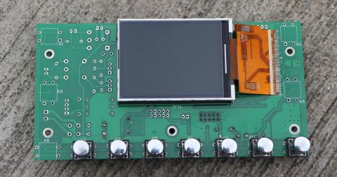
Rigid-flex designs can have multiple regions where the flex section branches. This might terminate at a connector, another rigid section, stiffener, gold fingers, or a circuit assembled onto the flex region. A complex example is shown below.

Rigid-flex PCB assemblies can have multiple branches and rigid sections.
Mechanical Constraints on Rigid-Flex Designs
Fixation
Rigid-flex designs often need to be fixed into the enclosure, which could be done with screws or snap-in mounts. Some fixation methods also use a slide-in bracket which holds the flex or rigid section in place. This commonly requires mounting holes to keep the rigid-flex assembly in place.
Permanent Deformation
In some rigid-flex assemblies, the flex ribbon is permanently bent or creased during installation so that the final board holds its shape inside the enclosure. These are static flex applications where the bend is applied once and the ribbon does not move again during operation. When this permanent deformation is planned, the designer should define the crease or fold region in the PCB layout using keepout areas. These keepouts prevent components, vias, and traces from being placed in the zone where the bend will occur, because copper features in a crease zone are subject to concentrated mechanical stress that can crack traces or fracture solder joints over time. Defining these keepouts early in layout, ideally informed by the MCAD model of the enclosure, ensures that the flex ribbon can be folded into its final position without unexpected interferences.
Bending Limits
The distinction between static and dynamic bending is the primary constraint that governs the minimum allowable bend radius in a rigid-flex design. Static bending occurs when the flex ribbon is bent once or a small number of times during installation and then remains in a fixed position for the life of the product. Dynamic bending occurs when the flex ribbon undergoes repeated, ongoing flexing during normal operation, such as in a hinge, robotic joint, or wearable device. The minimum bend radius is defined as a multiple of the total flex thickness in the bend region. For static flex applications, the generally accepted minimum bend radius is 6x the flex thickness, with 10x being a more conservative and widely recommended starting point. For dynamic flex applications, the required bend radius increases substantially, often to 100x the flex thickness, depending on the number of expected bend cycles over the product lifetime.
As a calculation example, consider an 11 mil thick four-layer flex region in a static application. Using the conservative 10x guideline:
Rmin = 10T = 10×11 mils = 110 mils
Using the bare minimum 6x guideline:
Rmin = 6T = 6×11 mils = 66 mils
If this same 11-mil flex region were used in a dynamic application requiring long cycle life, the bend radius would need to increase to approximately:
Rmin = 100T = 100×11 mils = 1100 mils
This illustrates how quickly the mechanical envelope grows when a flex region must survive repeated bending. Thinner copper weights (half-ounce or third-ounce), rolled annealed copper, and adhesiveless laminates all help improve bend life, but they do not eliminate the need to respect the bend radius constraint.
These bending limits create a direct coupling between the rigid-flex PCB stackup and the enclosure mechanical design. If the enclosure geometry is defined first, the available space for the flex ribbon to bend dictates the maximum flex thickness and minimum bend radius that the PCB designer can use. Conversely, if the stackup is defined first based on electrical requirements such as layer count, impedance, or copper weight, the resulting flex thickness imposes a minimum bend radius that the mechanical designer must accommodate in the enclosure.
In practice, this means the PCB stackup and the enclosure geometry must be co-developed. A four-layer flex region that meets the electrical requirements may be too thick to bend within the available enclosure volume, forcing a tradeoff between layer count, copper weight, and mechanical clearance. Early collaboration between the electrical and mechanical design teams, ideally through synchronized ECAD-MCAD collaboration tools, prevents late-stage conflicts where the flex ribbon physically cannot fit the enclosure without violating its bend radius limits.
Mechanical and Reliability Testing in a Rigid-Flex PCB
Once mechanical constraints are defined, typical reliability tests are often demanded for the design or the product as a whole. There may then be a question of how to validate the rigid-flex design mechanically.
EDA software does not provide this kind of validation directly. However, there are two ways to do this:
- Physical testing: the assembly can be put into vibration testing, environmental testing, etc., to verify the reliability of the PCB and the assembly
- Simulation: mechanical simulations can be used to understand the behavior of the assembly under vibration, mechanical shock, or other extreme conditions
For the simulation portion, it is possible to bring rigid-flex designs into MCAD software without relying on file exchanges. Commercial MCAD software can provide vibration, stress/strain, and assembly simulations on rigid-flex designs created in Altium Develop. Using the advanced MCAD CoDesigner feature, users can create a digital twin of their electrical design inside commercial MCAD software. A mechanical designer can then use this to create an enclosure, to check for interferences, and even place major components or define rigid-flex mechanical constraints.

The Advanced MCAD CoDesigner feature allows Altium users to instantly port their rigid-flex PCB layout into popular MCAD applications.
How to Include Mechanical Constraints
Mechanical constraints in rigid-flex designs typically involve locked placement of specific components and the use of keepouts. Sometimes, keepouts are based on the height of components so that there will not be interferences in an assembly. In PCB design software, these are defined using design rules and keepout definitions drawn directly in the PCB layout.
Defining Design Rules for Mechanical Constraints
Altium Designer provides a constraint-driven design rule system that allows mechanical requirements to be enforced directly during layout. Clearance rules, placement rules, and region-specific constraints can all be scoped to particular board regions, layer stacks, or component classes, which makes them well suited to rigid-flex designs where different zones of the board have fundamentally different mechanical requirements. The following steps outline how to set up design rules that support mechanical constraint definition in a rigid-flex layout.
- Design workflows range from object-centric spreadsheet interfaces to classic query-based rule engines for flexible scoping.
- Enforcement of mechanical requirements like clearance and region-style constraints is achieved through automated DRC and Room constructs.
- Signal integrity optimization involves precise termination, stackup-based impedance control, and evaluating channel losses using eye diagrams and impulse responses.
- Centralized library management reduces design risk by facilitating the reuse of validated symbols, footprints, and proven circuit blocks.
- Manufacturing readiness depends on early communication with fabricators regarding material availability, copper weights, and via aspect ratios.
- Integrated PLM and MRP systems improve traceability and supply chain visibility, helping teams manage complex product lifecycles and procurement volatility.
Using Keepouts in the PCB Layout
Keepout regions in a PCB layout define areas where specific objects such as traces, vias, components, or copper fills are prohibited. In rigid-flex designs, keepouts serve a structural purpose beyond standard clearance enforcement: they prevent copper and components from being placed in bend zones, crease regions, or areas that must remain clear for enclosure fitment. Keepouts can be drawn on specific layers or applied as multi-layer restrictions, and they are checked against the active design rules during DRC. The following steps describe how to define and apply keepout regions in Altium Designer for a rigid-flex layout.
- Define Scope: Determine if the keepout applies to all signal layers (using the Keepout layer) or a single, specific copper layer.
- Define Geometry: Place a Keepout Region over the rigid or flex area where routing and placement must be prevented.
- Set Restrictions: Configure the restrictions in the Properties panel to block specific object types (e.g., vias, tracks, pads) within the defined region.
- Verification: Confirm that automated routing and placement features are blocked according to the rules, preventing design violations in protected areas.
Whether you need to build reliable power electronics or advanced digital systems, use Altium’s complete set of PCB design features and world-class CAD tools. Altium provides the world’s premier electronic product development platform, complete with the industry’s best PCB design tools and cross-disciplinary collaboration features for advanced design teams. Contact an expert at Altium today!

About Author
Related Resources
Related Technical Documentation
Table of Contents
Design to Release, Without the Friction
- Keep reviews tied to the right version
- Reduce handoff confusion and rework
- Spot sourcing and release risk earlier
- Work solo, share when needed
Get Started
Thank you, you are now subscribed to updates.

