


Hatched Ground Plane Impedance Simulation in Flex PCBs

At a Glance
Flex PCBs can be high-speed PCBs too, but they need a hatched ground plane. Here are some tips for determining impedance on hatched ground planes.


Flexible PCBs and rigid flex PCBs can both carry high-speed signals, some of which demand controlled impedance. Implementing controlled impedance on a flex PCB is not a very easy task for several reasons. If you choose the controlled impedance route, where the manufacturer tests the impedance and makes adjustments to the stack up, you rarely have the freedom to do this as it may force the flex layer thickness to be too thick or too thin. If you go to the controlled dielectric route, the structure of the ground plane invalidates typical models for impedance, so it is very difficult to determine the appropriate impedance.
Unfortunately, this means that you must use some simulations or some test data to determine impedance of single traces and differential pairs in flex PCBs. Not all manufacturers can supply this data, or if they have this data, they may not make it publicly available. When it comes to differential pairs, the spacing will also be a critical factor that determines the impedance along the interconnect.
In this article, which is inspired by the work of Lukas Henkel, I'll present a brief set of simulation results and workflow that can be used for the determination of trace impedance on hatched ground planes.
Motivation for Hatched Ground Plane Impedance Simulation
Just recently, we completed a follow-up interview with Lukas Henkel, where we discussed some of his progress on the Open-Source Laptop Project. This project involved creating the motherboard as well as peripherals for an open-source laptop, and one of the peripherals is a webcam, which sits in the top part of the display. Take a look at our interview clip to learn more, or watch the entire episode on YouTube.
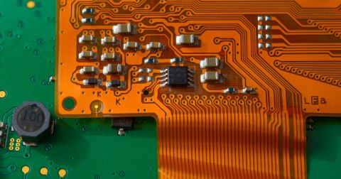
In referencing the webcam portion of the design in this clip, the webcam connects to the motherboard using a flex PCB. In order to route data from the camera to the CPU, a high-speed serial link is needed. This requires the use of MIPI CSI-2, a high-speed differential interface that sends serial data over four parallel lanes with a source synchronous differential clock. In total, this gives up to five differential pairs running between the camera and the motherboard.
CSI-2 routing over 4 data lanes and a source-synchronous clock lane. Both traces in each differential pair require length tuning, and the differential pairs must be matched within this group.
Being a differential interface, please use differential pairs requiring impedance control to 100 ohms. On a rigid PCB, this would be quite easy. Use the layer stack manager and Altium Designer or another simulator to quickly get the lossless impedance based on the stack-up cross-section. On a flex PCB, this is not so easy because flex PCBs use a hatched ground plane. Now, let’s briefly look at the theory showing why this is the case. Then, we can show some simulation results for Lukas’ flex ribbon, which will detail the differential impedance and differential S-parameters.
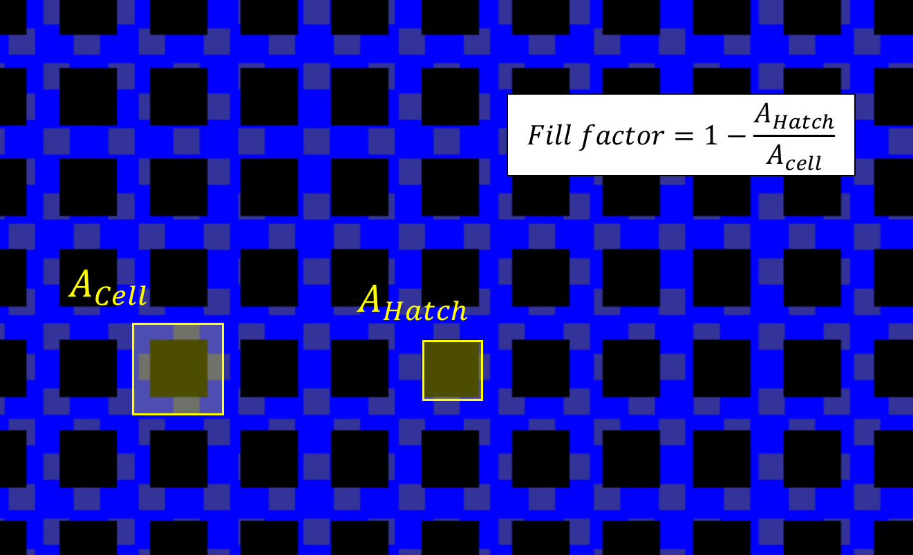
Fill Factor Is a Critical Parameter Determining Impedance
When evaluating the impedance of a copper interconnect on a flex PCB with a hatched ground plane, one of the tools we can use to understand what is happening in the interconnect is input impedance. If you look at the structure of the hatched ground plane, the hatch has some areas where copper is removed, typically square or diamond in shape, and that area can be defined as some fraction of the repeated area elements that make up the hatched ground plane. I've called this fraction the "fill factor," which can be defined as shown in the image below.
Now let us route a trace over different regions of the above structure; some portions of the trace will be over solid copper, while other portions of the trace will be routing over a region with copper removed. The varying presence of ground near the trace will impact impedance and thus signal integrity on these routes. Along the length of the trace, we would expect variations of high and low impedance, which will be a function of the trace-to-copper distance.
Because we have a variation in impedance along the length of the route, the structure is a periodically cascaded transmission line. I have not seen a good resource in the research literature specifically describing this type of structure, although I do make reference to it in this article. In any case, there is an input impedance in each section which can be written in terms of the next transmission line section:
In simpler terms, if you know the characteristic impedance of each of the transmission line sections, you could get a reasonable estimate of the S-parameters via an inductive calculation, and it would be simple enough to do in a Python script or in Excel. For example, if you knew the impedance above copper and in the hatch region, it is conceivable you could use the above equation iteratively to estimate the return loss (S11) at the input port.
I would submit that this method is more accurate than attempting to assume a solid plane and then applying some correction factor, but I think this is a subject for further study. In any case, once you have an estimate of the single-ended or differential impedance over a hatched ground plane, you will eventually need to qualify this, and that requires a 3D simulation.
3D Simulations of Hatched Ground Planes
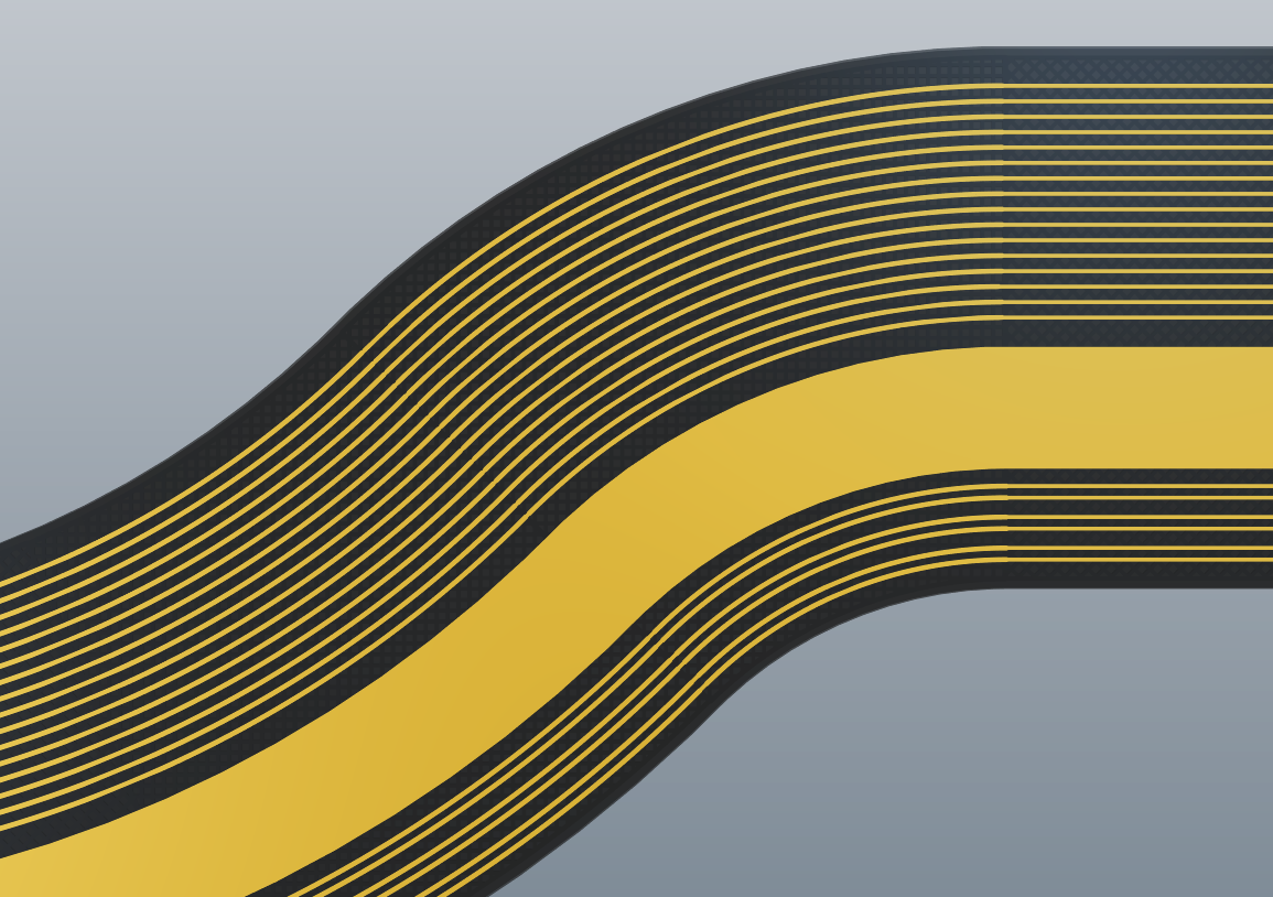
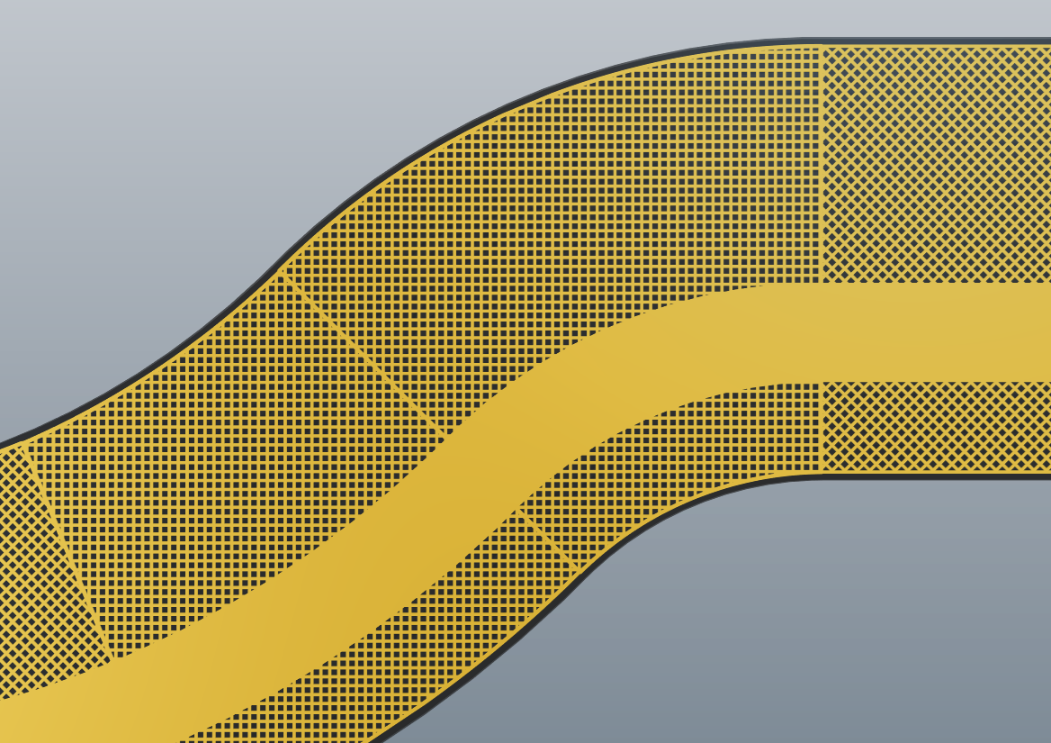
To more fully qualify the performance of interconnects on a hatched ground plane, we will use the flex ribbon shown below as provided by Lukas Henkel for the open source laptop. The image below shows a 3D view of the flex ribbon and trace routing in two regions, as well as the groups of traces in each region.
Layer 1:
Layer 2:
First, to get some values of the characteristic impedance in each section, the compliance analyzer in Simbeor is used to get impedances based on trace cross sections. Two regions were examined and compared. In the straight region coming directly from the camera connector, the impedance of the single-ended lines appears to exhibit much lower variation; the impedance varies from 30-40 Ohms along the straight runs. In the curved region of the flex cable, the impedance variation is much larger with characteristic impedance ranging from 30-60 Ohms.
The wide linewidth (W/H = 4) creates regions of very low odd-mode impedance over the copper, while regions between the copper are much closer to a 50 Ohm target. The exact variation appears to be approximately 28-62 Ohms, or an average of 45 Ohms odd-mode impedance. The differential impedance comes to approximately 78 Ohms with some variation.
Straight region:

Curved region:

Based on what we already see, there are some large impedance deviations along the link, although they are small in their length, so we would expect some mode conversion along this link. The full S-parameter matrix for this link will tell us the losses and mode conversion, and the results are shown in the next section.
CSI-2 S-Parameter Results
Now let's look at the S-parameters for the CSI-2 link as it is impedance controlled. Based only on the cross-section impedance values shown above, it becomes quite unclear what the actual return loss will be along the interconnect. Therefore, we run an S-parameter simulation from this geometry to determine the return loss up to very high frequencies. The image below shows the results for the CSI-2 lane highlighted above.
The return loss is acceptable within limits required for a CSI-2 link; the insertion loss is quite low within the channel bandwidth thanks to the width of the traces, but rolls off hard beyond the band limit. One problem here is mode conversion, specifically SCD21 (lower right graph), which we would expect given the discontinuous nature of the hatched ground plane. This link has a lot of mode conversion which would need to be checked against the MIPI C-PHY limits.

If you wanted to improve the return loss and insertion loss results, you would need to adjust the fill factor and spacing for the differential link. You would then need to simulate again and check to see that the S-parameters have improved. See the workflow section below for more details.
Summary of Results and Workflow
For our purposes, where we are just looking at the trace routing on the PCB, this result is acceptable. In reality, the S-parameters for the full interconnect will depend on impedance mismatch at the cable interfaces coming into connectors. To expand the simulation beyond what is shown above, we would need to do the following:
- Export a Touchstone file of the S-parameters for this link.
- Grab Touchstone files for the connectors at each end.
- Grab a Touchstone file for the link leading to the CPU and camera chip.
- Add all of these into a linear network model.
- Determine the S-parameters for the entire cascaded network.
- Depending on these results, one may need to adjust the fill factor for the hatched ground below the CSI-2 differential pair.
- Iterate and repeat.
The above process illustrates a workflow to be implemented for determining trace impedance for a CSI-2 lane. Due to the lack of accurate analytic results that could be used for prediction of trace impedance over a hatched ground plane, one needs to start with an estimate based on fill factor, and then iterate through some variations to get an appropriate trace impedance. I propose the following workflow:
- Start with a proposed hatching design and calculate the fill factor.
- Calculate two additional fill factors to be used as variations.
- Design a small test board with these variations and simulate S-parameters in each.
- Examine the S-parameter results and pick the best fill factor.
- For differential pairs, examine the result and determine if spacing should be adjusted to increase or decrease the differential impedance.
- Simulate the modified differential link and check the S-parameters.
- Iterate and repeat.
With these three simulations, and possibly a fourth based on adjusting the differential pair spacing, you could arrive at a usable interconnect design in only four simulations with approximately 8 hours of simulation time. This is fast enough to complete in a single day.
To provide more insight into the performance of single-ended and differential links over hatched ground planes in flex PCBs, I plan to do a larger geometry study. This will involve varying many of the fill factor parameters and determining which geometric parameter is the most effective estimator for single-ended and differential impedance. Make sure to follow this blog series for more updates.
Whether you need to build reliable power electronics or advanced digital systems, use the complete set of PCB design features and world-class CAD tools in Altium Designer®. To implement collaboration in today’s cross-disciplinary environment, innovative companies are using the Altium 365™ platform to easily share design data and put projects into manufacturing.
We have only scratched the surface of what’s possible with Altium Designer on Altium 365. Start your free trial of Altium Designer + Altium 365 today.

About Author
Related Resources
Related Technical Documentation
Table of Contents
Design to Release, Without the Friction
- Keep reviews tied to the right version
- Reduce handoff confusion and rework
- Spot sourcing and release risk earlier
- Work solo, share when needed
Get Started
Thank you, you are now subscribed to updates.

