


Gigabit Ethernet Switch Project


Gigabit Ethernet is now effectively an entry-level standard for office and commercial networking. There are many components available that can be used to build a simple Ethernet switch, but in this article, we will show an example design for a high port count Ethernet switch. The design shown in this article also includes an expansion for fiber optic cable with an SFP connector. This project requires successful implementation of several common aspects of high-speed design, including:
- BGA fanout
- Differential pair design
- AC coupling capacitor placement
- Designing with power planes in large BGAs
- Single-ended and differential high-speed interfaces
As usual, the project files can be downloaded from my website. You can also check out the download links in the Altium 365 viewer embed below. Click on this link to download a ZIP archive with the project source files or you can use the download link in the embed.
Main Components in the Gigabit Ethernet Switch
This Ethernet switch project is based on the VSC742x series of Ethernet switch processors from Microchip. These processors can be paired with an associated expansion PHY which connects to the switch processor over an SGMII interface. There are additional components for memory and external communication, as well as several power regulators. The list of main components in circuits includes:
- Main VSC7426 Ethernet switch processor and VSC8574 expansion PHY
- DDR2 RAM
- SPI flash memory
- RS-232 serial transceiver
- Enable toggle circuit for the fiber transceiver
- Connector for 12V input
- Power regulators for 3.3V, 1.8V, 1.2V, and 1.0V
In total, the device supports 12 standard Ethernet ports, includes one uplink port, and includes one SFP port for a fiber transceiver. The design also includes a serial interface brought onto an RJ-45 connector without the mag jack termination circuit.
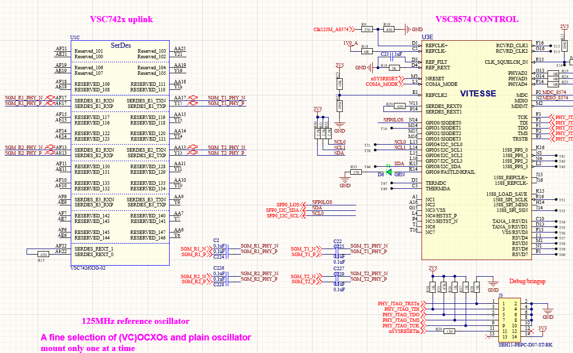
VSC7426 and VSC8574 Schematics
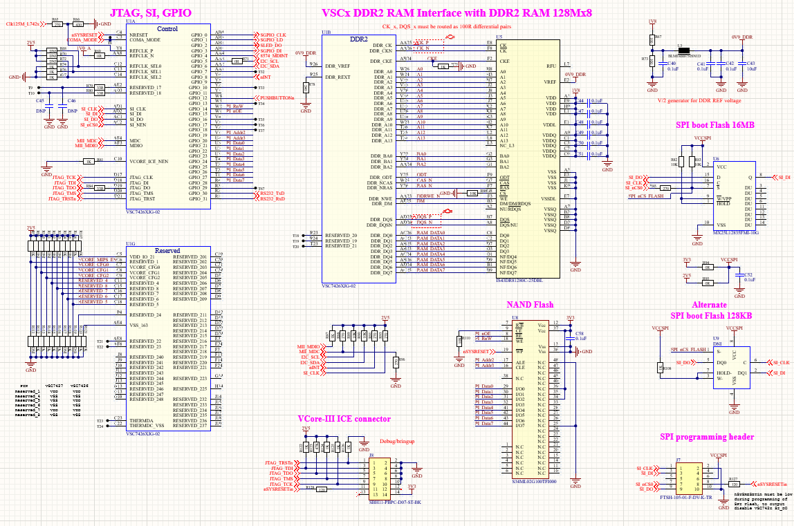
In the project files, the schematics for the switch and port interfaces are found on pages one, two, and three. The VSC7426 includes a DDR2 interface and uses an external DDR2 RAM chip. It has several GPIOs which can function as indicators, although the vendor-provided firmware also provides the required status messages on a terminal.
Schematics for this design are roughly based on the VSC7426/VSC7427 reference design from Microchip. You can access the original reference design on Microchip’s website.
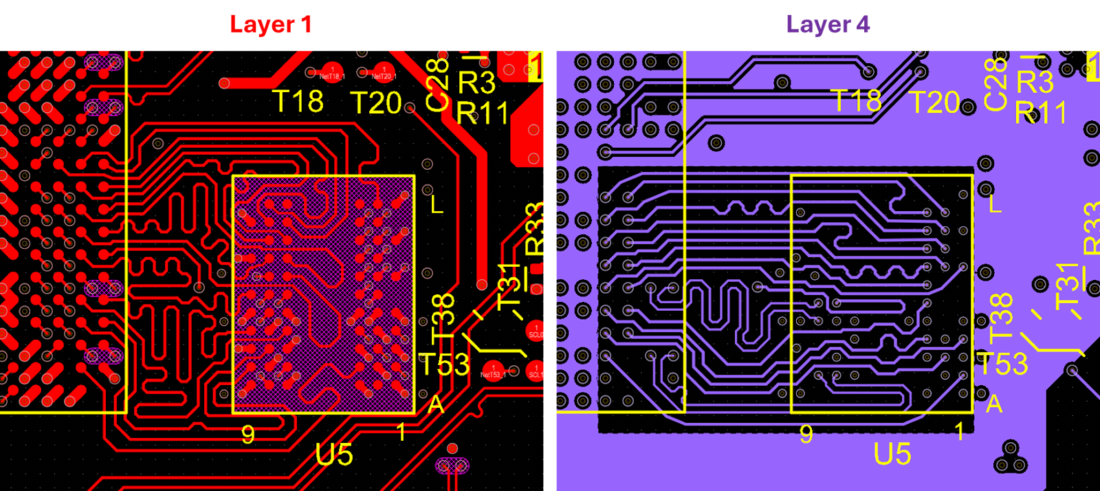
VSC7426 and VSC8574 circuits are shown in the images below. The VSC7426 is the star of the show and it provides up to 16 RJ-45 ports. The VSC8574 is used to expand this port count and communicates with the VSC7426 via an SGMII interface. AC coupling caps are included as is standard in SGMII. Note that Microchip’s documentation on this chipset recommends upgrading the VSC8574 to VSC8664; however, the publicly available embedded OS package is compatible with the VSC8574 chip.
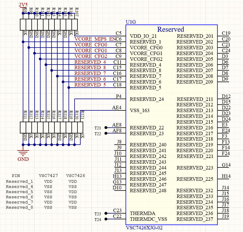
Some of the settings on the VSC7426 are determined through a set of configuration resistors on pins C6, C7, C8, and C9. The array of 1 kOhm resistors shown below can be installed or removed as needed to toggle various features on the VSC7426. The VSC7427 can also be used in this design but it requires changing some of the resistor settings, as detailed in the lower left corner of the image.
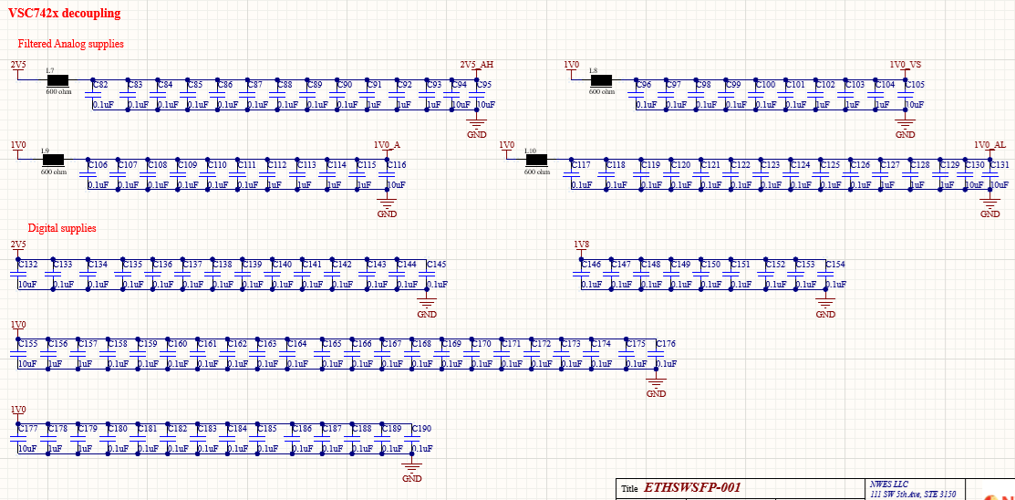
These chips have multiple rails and use a decent amount of power to generate clock and signal. As can be seen below, the chips use a significant number of decoupling capacitors to ensure power integrity.
You will notice that ferrites are being used for isolating elements due to high current consumption in the main logic supply. As has been mentioned in some other Altium articles, this approach sometimes works for isolating a slower PLL or analog rail from a fast digital rail running in parallel, but testing should be performed to confirm the ferrite does not amplify transients between the two rails. This is something I will discuss in more detail in an upcoming article and video, but in the meantime, I will refer readers to an older DesignCon presentation that discusses this specific use case of ferrite beads.
SFP Connector Circuit
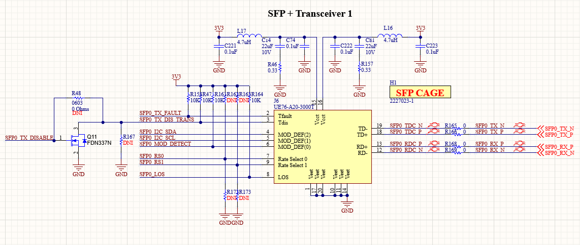
The image below shows the SFP connector circuit used to connect to a fiber optic transceiver. The SFP connector circuit shown here is used in other designs running up to 10 Gbps. The SFP connector requires multiple configuration resistors to access certain features on a fiber optic transceiver. Some of these have been marked DNI in the schematic below as they are not required for minimum viable functionality of the fiber optic transceiver.
In addition to the MOSFET used to toggle the Tdis pin, there is some additional logic between the VSC8574 and the MOSFET. One could bypass this additional logic if one wants to permanently enable the fiber optic transceiver. To do this, pull the MOSFET gate high or pole the enable pin low, and this will toggle on the transceiver.
Another important point here is the zero-ohm resistors on the RX and TX lines. The zero-ohm resistors could be replaced with AC coupling capacitors, but these are not required. The reason is that AC coupling is built into standardized fiber optic transceiver modules. When using this circuit at 1 Gbps, swapping between 0-ohm resistors and different AC coupling capacitor values will most likely not create any signal integrity benefit or detriment. If this schematic is to be used at higher data rates, the coupling capacitors and their location could be adjusted based on reasons I describe in this recent article.
RAM and Flash Memory
The design includes both flash memory and RAM for data storage and holding the firmware binary, respectively. The design includes two flash chips, as shown below, although only one of these is required for a minimum viable design. The smaller 128 Mbit Macronix NOR flash chip (MX25L12835FMI-10G) was used in our demo PCB and has been used in production versions of this design.
RAM and Flash memories found in SCH003.
The flash memory needs to be hooked up to SPI and will be written using an external programmer using an SWD connector. This will be discussed in more detail later.
There are two other memory chips which can be used in the design:
- U8: Infineon S34ML02G100TFI000 (2 Gbit parallel NAND flash)
- U9: ISSI IS25LQ010B-JNLE (1 Mbit NOR SPI flash, currently obsolete)
In our demo board, we have marked these DNI and they were not included in the assembly.
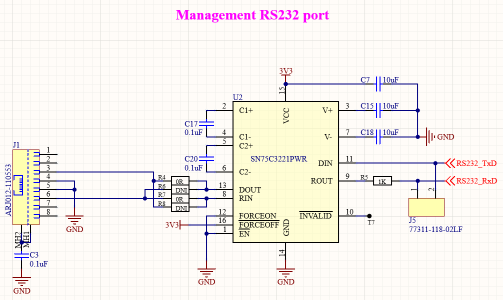
RJ-45 to Serial/RS-232
One way to quickly connect to an Ethernet switch installed in a rack is to use a serial port. To make the port accessible through the device enclosure, one option is to output a serial port over an RJ-45 connector. This is done below using a non-mag jack connector. Depending on the orientation of the RJ-45 serial port, a cable could be routed to a patch panel, and a technician could then plug their computer into a patch panel to access the serial port.
Serial port access was also added using a two-pin header on the input of the RS-232 transceiver (J5 in the above image). This gives you serial port access over a USB-to-UART module.
PCB Layout
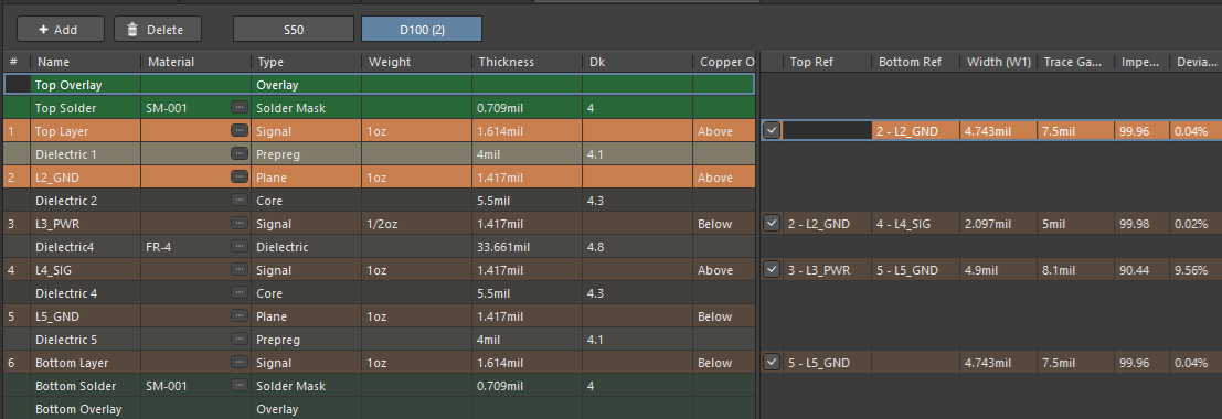
This design has three BGAs in total, with the largest BGA being the VSC7426 with 672 pins. Most of the pins on the VSC7426 and the VSC8574 are ground and power, so we will not need a very high layer count board to complete the routing. This board was completed using six layers with the stack-up shown below.
PCB stackup and impedance settings
This stack-up nearly matches a standard stack-up from JLCPCB, although the tolerances on DDR2 and Ethernet allow some variation in the layer thicknesses. As long as the outer layers are thin and the inner core layer is thick, the differential impedance and single-ended impedance of the impedance-controlled lines hit the target impedance within the allowed tolerances. The thin outer layers ensure that our microstrip routing will not be too wide, as the Ethernet lanes and DDR2 lanes require controlled impedance.
All differential pairs in the design were routed with 100-ohm differential impedance. Although the stack-up was custom-designed to be produced at a wide range of fabrication houses, the demo board shown later in this article was produced at JLCPCB with one of their standard stack-ups.
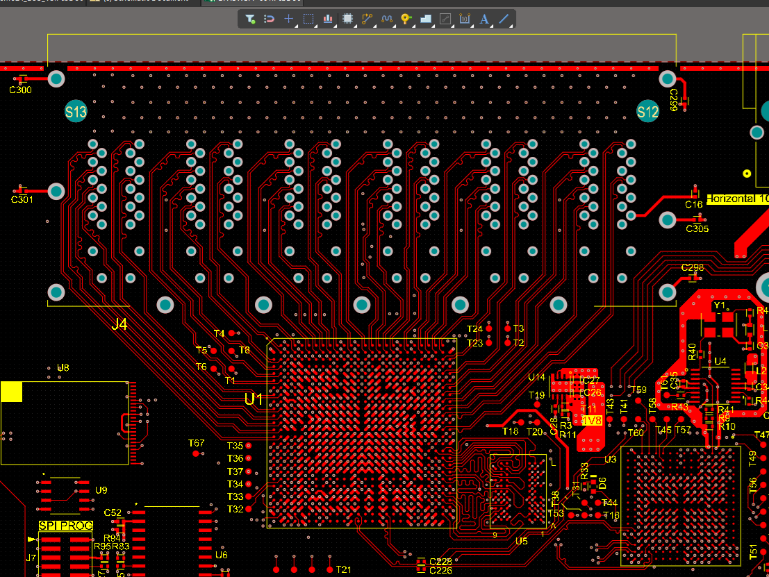
BGA Fanout
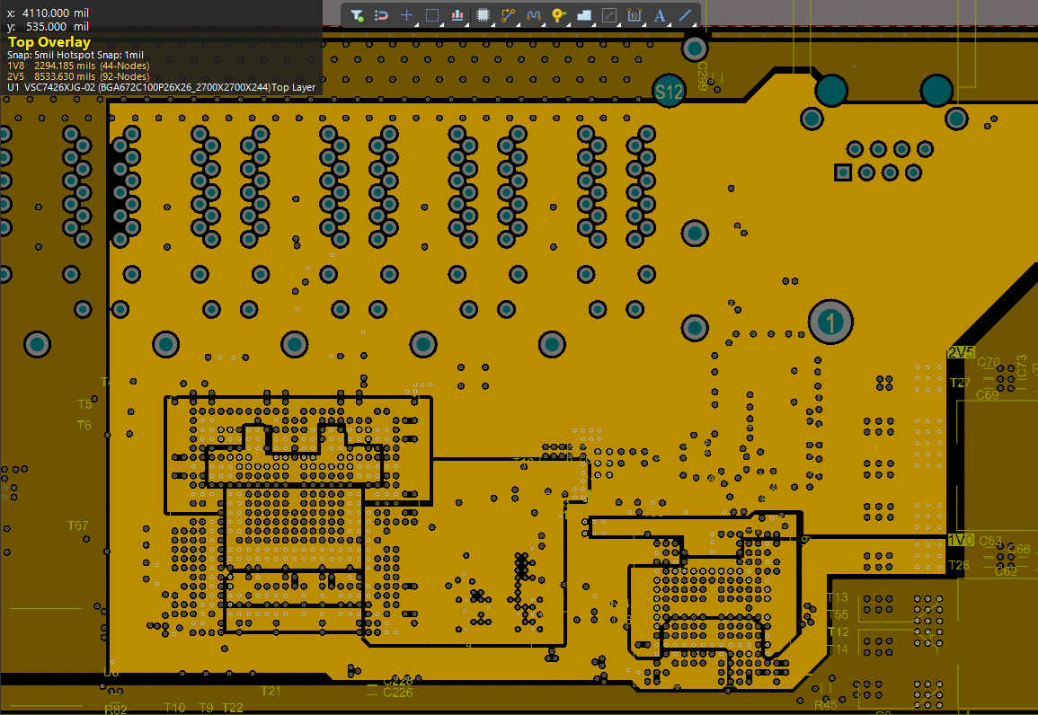
The Ethernet PHY chipset and the DDR2 chip have ball pitches of 1.0 mm and 0.8 mm, respectively. This means we can use through-hole vias with dog-bone fanout to reach the inner rows of the BGAs. We also do not need blind and buried vias for the Ethernet links because the VSC chips have the Ethernet pins clustered around the edge of the packages. This means the Ethernet lanes can be routed straight into the packages as differential microstrips. This routing is shown below, including small length tuning sections where corners are present in the routing.
DDR2 Routing
Next, the DDR bus is wide enough that the design requires two layers to fully route into the DDR chip. This is shown in the two screenshots below. The DDR bus is routed with 50-ohm impedance on the internal layer and external layer; the differential clock is shown on Layer 4.
It is perfectly acceptable to perform this type of routing for a parallel bus, but it requires delay tuning across the outer and inner layer. Because microstrip propagation delay is determined by an effective dielectric constant, signals traveling along a microstrip and stripline will have different propagation speeds. This requires delay tuning on the different layers to ensure all the signals on the DDR2 bus arrive within the required time window.
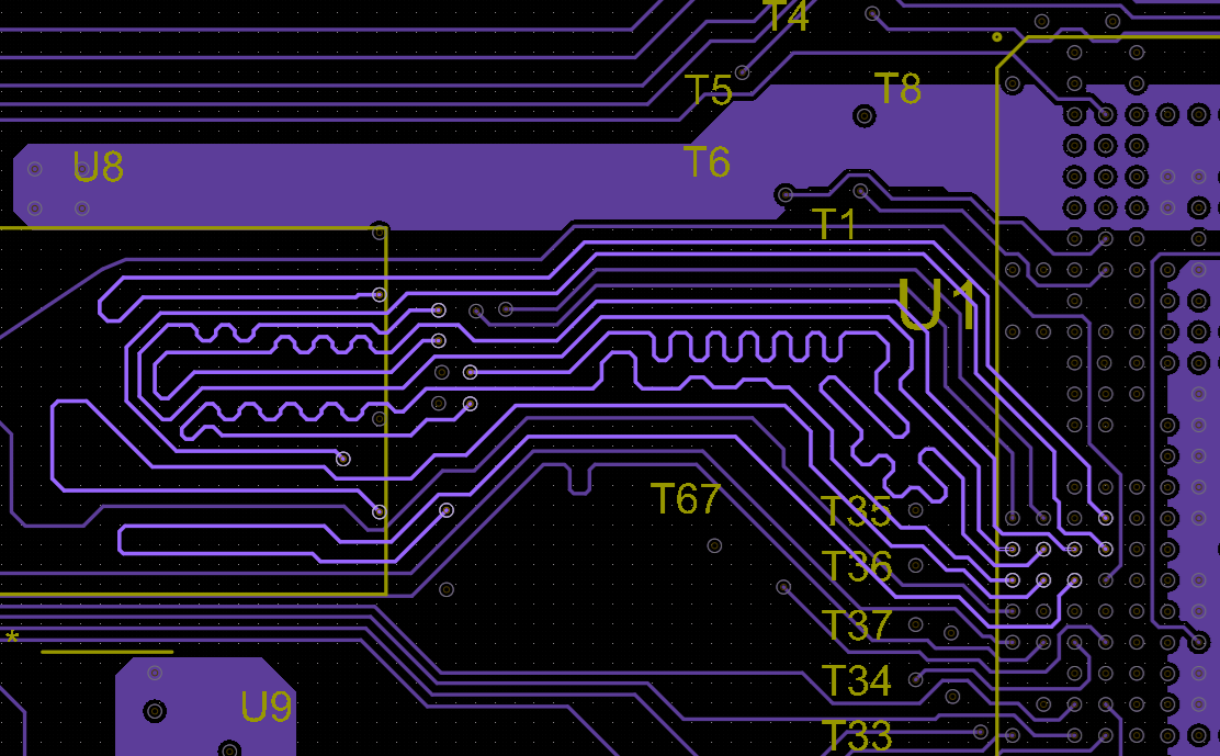
Parallel Interface
The parallel interface NAND flash was not installed in the demo board, but the design does accommodate it if needed. The parallel interface uses 8 length-matched traces to route between the VSC7426 and the parallel flash. This routing is confined to Layer 4 and is shown below (the parallel interface is highlighted).
Power and Grounding
Because this design involves a processor that has many high-speed I/Os operating simultaneously, some basic power integrity principles need to be implemented. In the schematic, we showed a large number of capacitors being used on the logic rails, but the PCB also needs plane capacitance for power stability in the 100 megahertz range. This requirement for power stability applies here because the Ethernet interfaces being supplied in this device have channel bandwidth requirements in the 100 MHz range, so we need to ensure stable power at least up to these frequencies.
To do this, we route large rails on Layer 3 to supply power directly to the high-speed I/O supplies at 3.3V, 2.5 V, 1.8 V, and 1.0 V.
To ensure that the design has low inductance on the connections for each capacitor, all the small bypass capacitors were mounted directly on the back side of the PCB, behind the VSC7426 BGA package. A direct connection through a pair of through-hole vias to balls on the BGA package adds approximately 1 nH of inductance to the capacitor ESL value and it will limit the response capability of small case SMD bypass capacitors to the 10 MHz range. The same approach was taken on the VSC8574.
Decoupling/bypass capacitors are connected directly to the through-hole vias on the power/ground pin pairs to ensure low inductance connections on the capacitors.
Together, the bulk capacitors on power supplies, bypass and decoupling capacitors on the BGAs, the plane capacitance from the large rails, and on-die capacitance in the Ethernet chipset collectively cover up to the GHz range and help ensure power integrity.
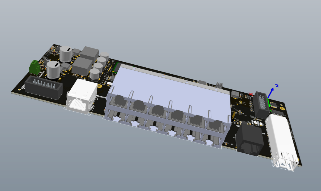
3D Model
The complete 3D model of the finished PCB layout is shown below. We can see the 12x RJ-45 ports, the additional GbE Uplink port connected to the VSC8574, the serial-RJ-45 connector, and the SFP cage for our fiber transceiver.
Programming and Bringup
The VSC7426 runs an embedded Linux kernel using RedBoot as a bootloader. The embedded OS is straightforward to install and the code is available from Microchip. The vendor makes different versions of the code available depending on the master clock frequency, expansion PHY, and configuration settings used in the design. To help readers get started quickly, I have included a working firmware binary in the project files.
To flash the binary onto the device, users will need a programmer with a SPI interface. The programmer I prefer to use for flashing is the Forte programmer, which is available from ASIX.net. This programmer supports a long list of microcontrollers and memories, including the Macronix SPI NOR flash used in this project. The video at the end of this article outlines the flashing steps using the ASIX UP programming software and the Forte programmer.
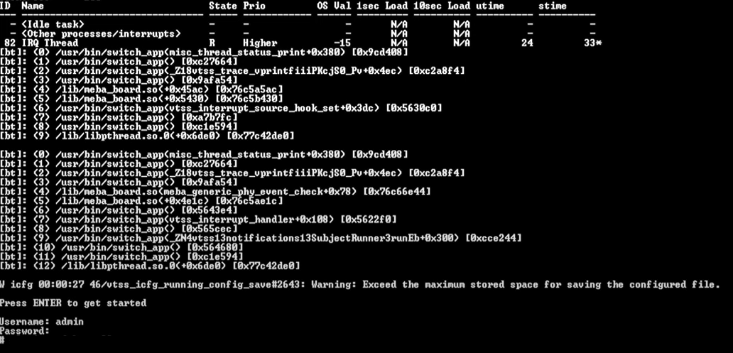
Once the flashing process completes, power down the design, unplug the programmer, and connect a serial bridge to the 2-pin header (J5) to access the UART interface (115200 kbps baud rate). Next, reapply the input power and the design will boot up to a login prompt; login with the username admin, the password is blank.
Terminal output (in TeraTerm) once the switch boots and the user logs in
There are further instructions required to fully bringup the design and active each of the ports. To complete these tasks, instructions can be found in the “VSC5611EV Mechanical Assembly and Programming Guide.pdf” file in the Binaries folder in the source files. The programming instructions start on Page 18 of the PDF file.
Full Project Overview on Altium Academy
The video below shows our bring-up work and a review of the PCB design on the Altium Academy Youtube channel. To learn more about this project and to see the process for flashing, you can watch the following video.
Whether you need to build reliable power electronics or advanced digital systems, use the complete set of PCB design features and world-class CAD tools in Altium Designer®. To implement collaboration in today’s cross-disciplinary environment, innovative companies are using the Altium 365™ platform to easily share design data and put projects into manufacturing.
We have only scratched the surface of what’s possible with Altium Designer on Altium 365. Start your free trial of Altium Designer + Altium 365 today.

About Author
Related Resources
Related Technical Documentation
Table of Contents
Design to Release, Without the Friction
- Keep reviews tied to the right version
- Reduce handoff confusion and rework
- Spot sourcing and release risk earlier
- Work solo, share when needed
Get Started
Thank you, you are now subscribed to updates.

