


How Does the Package PDN Impact Power Integrity?

At a Glance
Component packages have their own power distribution network (PDN) that influences their operation and drives compensation in the PCB.


Whenever we say something to the effect of “components can’t work without a correctly designed PCB,” we only have to look at component packaging for evidence. It is true that component packages come with parasitics that affect signal integrity, but there is one area that we don’t often look at in terms of component packaging: power integrity.
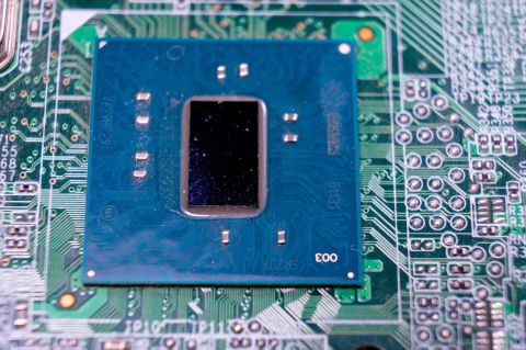
Every component package and semiconductor die has its own PDN, and when the on-chip structure is included in a PDN simulation, it becomes clear that the chip’s structure will influence power integrity. In addition, in advanced packages and modules built on substrates and interposers, certain components included in the package will affect power integrity, including everything from on-chip capacitance to an active power management die.
In this article, I’ll take a look at how the PDN in component packaging affects design practices for PCB designers. Below, readers will also find a typical model describing the PDN in a PCB that also accounts for the packaging of the load component in the PCB.
Effects of the Package PDN
Just like any element we include in a PCB, the package PDN has capacitive and inductive behavior that affects its electrical response to a fast pulse. When an integrated circuit is added to a PCB, these package parasitics change the PDN impedance spectrum as measured on a test vehicle. The result is that we have three PDN impedances:
- Off-chip: the PDN impedance only on the PCB, inclusive of all planes/rails, the voltage regulator, capacitor banks, and vias
- On-chip: the PDN impedance only on the chip, inclusive of all on-die planes, capacitances, contacts (bumps), and vias
- Equivalent PDN impedance: the total impedance of the chip + board when the two models are cascaded together
The on-chip PDN impedance can be determined by de-embedding its Z-parameter matrix from measurements of a (chip + board) test vehicle. In other words, once the chip is placed onto the board, the two impedances combine to provide the equivalent impedance spectrum. This is the actual impedance spectrum that produces the PDN impedance response at higher signal bandwidths reaching into the GHz regime. We can determine the response region where the on-chip PDN impedance matters by looking closer at typical impedance spectra in the chip and board independently.
Example Board and Package PDN Impedance
The two graphs below show an example of the PDN impedance for a PCB, and the PDN impedance spectrum for an advanced 3D integrated package being probed at various points. In this example package, multiple chips are stacked on an interposer and connected with through-silicon vias. The graphs are quite different, as will be described below.

The equivalent impedance is essentially the two impedance spectra for the board and chip placed as cascaded networks (e.g., in parallel, see the model below). This means that the on-chip PDN impedance will dominate the impedance spectrum at 1 GHz and above, and so the power rail ripple observed in the board will depend on the bandwidth contributions from each portion of the system.
There is an important consequence of this fact:
|
|
When armed with this information, where can a PCB designer focus their energy to ensure the board operates below the target PDN impedance within their required bandwidth? For this it helps to look at the components of a PDN in the package and in the PCB.
Board + Package PDN Impedance Model
I’ve covered the board-level PDN impedance in other articles, principally in this recent article. A model that includes both the PCB and package contributions to PDN impedance is shown below.

This model accounts for a package with a single die; a package with multiple dies (either 2.5D or 3D integrated) would include these dies in parallel connected with their own inductive interconnects through bumps. The on-chip capacitance could be bulk capacitance built into the die (package power planes) as well as on-chip capacitors, such as you would see in CPU packages.
At the highest frequency end of the PCB’s PDN impedance, we can see that the plane capacitance dominates. This is because it will have lowest inductance and it tends to have somewhat low capacitance. In order to decrease the impedance
- Use physically larger planes
- Use thinner separating dielectric between power and ground
- Use a higher Dk dielectric, such as an embedded capacitance material
These measures will increase the plane capacitance but will decrease the plane inductance. Therefore, you can likely bring down the PDN impedance curve between 100 MHz and 1 GHz with these measures when you need to supply power for very high bandwidth signals.
What’s Happening in the Package?
Inside the package for an advanced component, we see a few major characteristics that determine power integrity in a system beyond 1 GHz bandwidths:
- Package power/ground plane pairs
- Ball/via and bumps
- On-chip capacitors used in the package
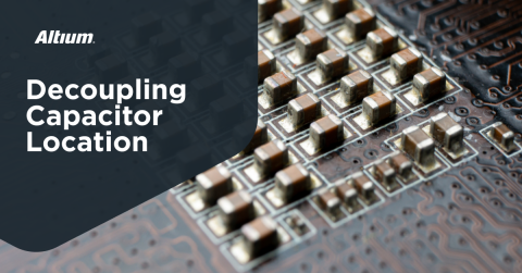
Some packages will include power management circuitry that includes a set of in-package capacitors and on-chip capacitance formed in deep narrow trenches in the silicon die. In some CPU packages, the approach is to put these components on the package substrate and connect them directly to the die to minimize loop inductance and spread the operating bandwidth well into the GHz range. This is almost identical to the way you would place decoupling capacitor connections to a BGA.

Beyond 1 GHz, the packaging designer is ultimately in control of the package PDN impedance and whether the power rail will exhibit strong noise in the GHz range. As a PCB designer, you have no control over what happens in the package PDN unless you take a direct role in designing the substrate, interposer, and interconnect architecture inside the package. This is not the typical role PCB designers play, although it is possible this will begin happening in the future.
When you’re ready to create a PCB stackup and layout that provides strong decoupling out to GHz frequencies and thus stable power delivery, use the complete set of product design tools in Altium Designer®. The CAD features in Altium Designer enable all aspects of systems and product design, ranging from packaging and PCB layout, and up to harness and cable design. When you’ve finished your design, and you want to release files to your manufacturer, the Altium 365™ platform makes it easy to collaborate and share your projects.
We have only scratched the surface of what’s possible with Altium Designer on Altium 365. Start your free trial of Altium Designer + Altium 365 today.

About Author
Related Resources
Related Technical Documentation
Table of Contents
Design to Release, Without the Friction
- Keep reviews tied to the right version
- Reduce handoff confusion and rework
- Spot sourcing and release risk earlier
- Work solo, share when needed
Get Started
Thank you, you are now subscribed to updates.

