How to Use SFP Connectors in Your PCB Layout
SFP connectors are used to route data into fiber optic transceiver modules, which are normally found in high-speed networking equipment. Today, however, I’ve had multiple design requests that involve the use of fiber transceivers outside of a data center environment. Newer systems in sensor fusion, MIMO systems, rugged OpenVPX switches, and some industrial robotics need to stream huge amounts of data back to a workstation or server, with data streams easily exceeding 10 Gbps per lane.
Streaming this much data from a small embedded device demands either a fiber transceiver or a bundled mini coax interconnect. The latter is still a bulky connector over copper, so I’m not surprised that engineers are requesting an SFP form factor for production grade systems. As I expect to see more of this going into the future, I decided to prepare this brief guide on the correct usage of SFP connectors and transceiver modules that target these very high data rates.
Getting Started With an SFP Connector
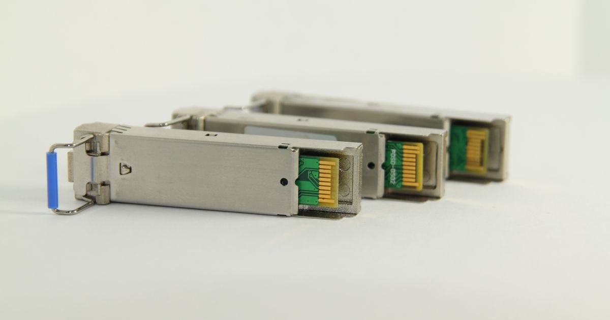
The small form factor pluggable (SFP) connector is designed to connect directly to modules that interface with copper or fiber. These are generally used with fiber links in the data center, although these links are now being found elsewhere as I mentioned above. The connector is designed to provide a hot-swappable interface for transceiver modules like the Cisco 10G module shown below.

SFP Connectors Types
The module includes a set of contacts along the edge that plug into the SFP connector, and the SFP connector will mount to the PCB as a standard SMD component. There are multiple types of SFP connectors that connect to transceivers with different data rates:
- SFP - 20 pin connector supporting a variety of speeds
- SFP+ - Same as SFP but supporting up to 16 Gbps
- SFP28 - Also 20 pins, but in an alternative form factor and supporting higher data rates
- SFP56 - Same as SFP28 but with higher speed limit
- XFP - A 10 Gbps pluggable connector with larger form factor and 30 pins
- QSFP - These devices have similar functions as in the above list (including its variants), but these connectors use 4 Rx/Tx lanes for much faster aggregated data rates
- QSFP-DD - The "DD" in this connector name stands for "double density" referring to the use of 8 Rx/Tx lanes instead of 4 Rx/Tx lanes
All SFP modules are designed for only one type of connector are not compatible with another type of connector. SFP modules are no longer the industry standard for the absolute fastest data rates used in Ethernet standards. Today, QSFP connectors are the dominant connector style used at faster data rates, e.g., at 100G Ethernet, as they aggregate multiple lanes into a single transceiver module. The newest Ethernet standards being implemented (with 224G-PAM4 data rates as of 2025) use QSFP-DD connectors with 8 lanes aggregated into a single transceiver.
SFP Connector Example Schematic
The embed below shows a schematic sheet for an SFP connector and the associated circuitry. The schematic gives the minimum viable circuitry required to operate an SFP transceiver. The configuration pins are primarily controlled through pull-up/pull-down resistors or an external signal, but typically these values are set statically and only the resistors are necessary. The MOSFET portion of the circuit is technically only required in order to toggle the transceiver on and off with a GPIO.
An important point in the above schematic is the use of the zero Ohm resistors on the differential Rx and Tx lines. These zero Ohm resistors can be swapped out for AC coupling capacitors so that coupling signal integrity in the channels can be adjusted based on the capacitor size. Note, however, that we have tested this schematic in multiple projects with and without the AC coupling caps, and the links are shown to function up to 10 Gbps.
The pin list and pin functions are shown below. Some of the pins are output pins which are readable by the system host, and some are inputs (such as the I2C pins) which are used to configure the SFP module.
|
Pad |
Name |
Function |
|
1 |
VeeT |
Transmitter ground |
|
2 |
Tx_Fault |
Output: transmitter fault indicator |
|
3 |
Tx_Disable |
Optical output disabled when high or floating |
|
4 |
SDA |
I2C interface data |
|
5 |
SCL |
I2C interface clock |
|
6 |
Mod_ABS |
Output: module absent indicator |
|
7 |
RS0 |
Rate select 0 |
|
8 |
LOS |
Output: receiver loss of signal indication |
|
9 |
RS1 |
Rate select 1 |
|
10 |
VeeR |
Receiver ground |
|
11 |
VeeR |
Receiver ground |
|
12 |
RD- |
Inverted received data |
|
13 |
RD+ |
Received data |
|
14 |
VeeR |
Receiver ground |
|
15 |
VccR |
Receiver power (Max. 300mA@3.3V) |
|
16 |
VccT |
Transmitter power (Max. 300mA@3.3V) |
|
17 |
VeeT |
Transmitter ground |
|
18 |
TD+ |
Transmit data (positive polarity) |
|
19 |
TD- |
Inverted transmit data |
|
20 |
VeeT |
Transmitter ground |
SFP transceiver modules communicate with the system host via the I2C interface. The system host can access the internal registers at addresses A0h and A2h in order to read device information, monitor status, or configure settings. A system can be configured to read the Vendor Name and Part Number, and based on the reading the system could reject or accept certain modules.
In the guidelines that follow in the next section, note that the VccR pin is referenced to a receiver ground pin; this means the VccR pin must be bypassed to the VeeR pin. The natural choice based on the pinout is to bypass Pin 15 (VccR) to Pin 14 (VeeR). The same applies to the transmit power and ground pins (VccT and VeeT, respectively), so the natural choice is to bypass Pin 16 (VccT) to Pin 17 (VeeT).
SFP Connector Layout Example
In the layout example I’ll show below, I’m using a standard 20-pin SFP connector for a 25G link over fiber (up to 100 m length). The same strategy can be used with the other types of SFP connectors with higher pin counts listed above, as well as QSFP connectors for 4-channel modules.
These modules include low-speed and high-speed digital interfaces, as we can see on the example SFP connector layout for a 10 Gbps transceiver module:

The important points in the layout are as follows: on the right, we have an I2C interface and some control signals. All of these are low speed and should generally be routed away from the high-speed differential pairs coming to the left side of the connector. Copper pour was used for balancing in this particular board, but this is not a requirement for the transceiver to function properly.
Next, the high-speed signals enter from the left side, and they are surrounded by GND and PWR pins. The Rx and Tx input/output differential pairs on L1 are marked with yellow arrows:

These lines are passing into the inner layers using differential vias, the vias drop down to L6 in an 8-layer PCB. Because the outer two dielectrics are thin (11 mil total thickness), the stub length is already minimized on this via transition and backdrilling is not needed. The differential pairs pass through an optimized antipad that sets the required differential impedance to 100 Ohms up to a bandwidth of approximately 10 GHz.

At very fast data rates, where multiple lanes are aggregated into a single QSFP connector, the connector body itself may become apparent as the main factor limiting data rate. Connector manufacturers have made efforts to qualify their components against target data rates, but of course those data rate targets might not be hit fully when the lines on the PCB are routed into the connector. A transmission line simulation program like ADS or Simbeor would be needed to fully qualify these channels when interfacing with a QSFP connector.
Power Integrity in SFP Connectors/Modules
It’s important to remember, optical transceivers are sending out fast pulses into an optical fiber, so they function just like any other high-speed digital component. This means we have to worry about power integrity on the power bus for these connectors. The typical guidelines for high-speed digital PDN design apply to SFP connectors as well.
In the above example, the incoming power is passed through a low-pass filter based on test data from our partner on the above project. Be careful with this approach as placing pi filters on a power pin for a high-speed component creates two possible outcomes:
- Excitation of a very strong transient if the filter is not critically damped
- Excessive filtering at high frequencies, causing the Rx lanes to transmit data which cannot be read by the system host
If you can't prove the filter works or the filter prevents your transceiver Rx/Tx lanes from operating correctly, consider just using more capacitance to suppress rail noise.

SFP Connector Cages
The images above just show an SFP connector mounted directly to the PCB as a simple connector. The optical transceiver module would then connect to the board along its edge, and the transceiver would show through the enclosure. This is fine if the enclosure has some method to fix the module into the enclosure so that the module is stable. The connector shown above could also be moved back away from the edge of the board so that fiber interface is closer to the board edge, as would be the case where the enclosure has a tight fit to the board edge.
In many pieces of networking equipment, the SFP connector will not usually hang off the edge in this way. Instead, the optical transceiver module will connect to the SFP connector through a cage. These cages are simple metal cages that are placed around the SFP connector, and they can hang slightly over the board edge. The enclosure is then built around the SFP connector cage so that the transceiver can be accessed through the opening in the enclosure. SFP connector cages are not required, but for systems that will take advantage of hot-swappable capability, it is recommended to include a cage. The cage provides the mechanical stability these transceivers need and it guides the transceiver module into the plug.
The image below shows an example of an SFP connector cage (Molex 74737-0009). These cages are through-hole mounted (press fit) connectors that sit near the edge of the PCB.

These cages are just metal enclosures that sit on the PCB, they do not have an SFP connector built into them. Instead, the SFP connector is available as a separate part number. These parts are interchangeable across vendors. Because the SFP cage and SFP connector are standardized, the SFP connector actually sits inside the cage along the back edge. This then leaves space for the transceiver to slide through the front side and connect to the SFP connector.
What does this look like in a PCB layout? The example below shows how the two components are placed. In the PCB layout, the cage is placed first; a good footprint will have a line marking the board edge in the 3D body layer or in the Assembly layer. In the example below, I've lined up the cage along the board edge. The SFP connector is then placed inside the cage along the back edge.

The connector must be very precisely placed inside the cage, otherwise the transceiver will not fit into the plug and the cage would need to be removed. To get the connector into the cage, the connector is placed first, and the cage will be mounted over the top of the connector. The cage has an opening in the back that allows the board-mounted connector to sit inside the cage. To ensure the connector is placed correctly relative to the through-holes for the connector, read the mechanical drawing for the connector; this drawing will show how to line up the pads and mounting holes for the SFP connector.
The image below shows the above SFP connector + cage pair in 3D; the view is looking into the connector from the board edge. As you can see, the cage is hanging over the edge of the board. This should illustrate the advantage of STEP models in your PCB design software; you can verify the orientation, spacing, and potential interference between these elements in the PCB layout.

Thermal Issues With SFP Connectors
The placement and layout are of course important to understand, but the other important aspect of using fiber optic transceivers with SFP connectors. Due to the power consumed in these connectors, one of the major issues at higher data rates is the power consumed by a fiber optic transceiver module. With over a dozen W being consumed during operation with faster protocols intended for very long distance transmission over fiber, there will be a lot of heat to deal with.
Unfortunately, because the transceiver is basically suspended above the PCB by the SFP connector, there will not be any direct contact to the PCB to dissipate that heat. You can take a few steps to help dissipate heat:
- Use a transceiver module with an integrated heat sink
- Mold the enclosure to make greater contact with the body of the module
- Consider adding a fan behind the module
This brings up another advantage of an SFP connector cage: they can provide a heat sinking function. Because these components are just sheet metal connectors, and they are connected back to the plane on an internal layer, they provide a mechanism to dissipate a lot of heat away from a hot transceiver. This heat would be dumped into the internal plane and the enclosure, and it could eliminate the need for more aggressive cooling measures like fans.
Whenever you need to place and route high-speed signals into an SFP connector in your PCB, use the 2D and 3D CAD tools in Altium. When you’ve finished your design, and you want to release files to your manufacturer, Altium makes it easy to collaborate and share your projects.


