


How Much PCB Mask Expansion is Too Much?

At a Glance
Solder mask expansion on a PCB can be set in your design rules to ensure sufficient copper is visible for soldering.


Even if you aren’t using top-of-the-line design software, you’ll still notice something very important in your PCB footprint layers: solder mask and paste mask openings. These will be placed into stencils and used to fabricate and assemble your PCB. With designers sometimes finding themselves needing to create their own components, it’s worth asking, what is the right value for mask expansions to set in your PCB footprint? The next question that comes up is: can this number be changed later?
This is actually quite an important design rule and it is something that should not be left up to guessing. While there are default rules for expansion values built into PCB design applications, there are many instances where these need to be changed for more advanced designs.
Your PCB Mask Expansion Setting
If you look at your PCB footprint in a layout editor, there will be data in two layers superimposed on top of the SMD pads for your parts. You can see this in the image below for an SOIC-8 footprint in a PCB layout.

Here you can clearly see that the paste mask layer (gray) is slightly smaller than the solder mask layer (purple), and the paste mask layer overlaps perfectly with the pad outline.
Are these values too large or too small? The best PCB design software will help you live your design life in easy mode, meaning you usually don’t need to adjust the mask expansion values. In other cases, the mask expansion absolutely needs to be changed, and typically you would need to make it smaller, not larger.
The “Easy Mode” Setting
Whether you are setting the mask expansion as static in the PCB footprint, or you adjust it manually with the PCB design rules, there is a setting that can make things easy for you. These settings might be set as the default paste mask expansion and solder mask expansion values. A reasonably safe approach is to do this following:
-
Set your paste mask expansion to be 0 mm/0 mil (paste mask opening equal to pad size)
-
Set your solder mask expansion to be any value larger than your paste mask expansion
-
The mask expansion should not exceed your pad-to-copper spacing values
If you take this approach and always set the paste mask expansion to 0 mil, and leave the solder mask expansion at the default value, you’ll usually be just fine. This works well if you are not working on anything too dense, where you have a lot of space between components so that you won’t create tiny solder mask slivers. When things do get very dense, it now becomes important to adjust the mask expansion.
The “Hard Mode” Setting
These settings are normally implemented when you have high-density component placement and routing. In this case, you may need to reduce the difference between the paste mask and solder mask expansion. The safest setting here, when high density component placements are used, is to set the solder mask expansion to no 1 mil. This will ensure you get maximum solder mask opening despite layer-to-layer misregistration.
This will also allow for fine line routing near SMD pads without exposing the nearby track to solder. In the example below, the default expansion value has been used on a standard pitch BGA, but this is in danger of exposing tracks in the escape routing region. Therefore, in these pads, it’s best to reduce the mask expansion to 1 mil, or possibly to 0 mil to help confine solder onto the landing pads.

Make Use of Your Design Rules
The simplest way to create your footprints to ensure you can access the easy mode and hard mode settings is to take advantage of your mask expansion design rules.
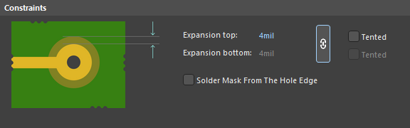
First, create your footprints with default mask expansion values on pads by configuring pads to follow the design rule setting. Then, when the part is imported into the PCB layout, the mask expansion values can be adjusted by changing the expansion value design rule. In Altium Designer, these values are adjusted using the “Solder Mask Expansion” and “Paste Mask Expansion” design rules.
Learn more about mask expansion settings in the Altium Designer documentation.
Even if you have to guess at the right mask expansion settings to use in your PCB footprints, you can quickly modify your settings later when you use the unified design environment in Altium Designer®. To implement collaboration in today’s cross-disciplinary environment, innovative companies are using the Altium 365™ platform to easily share design data and put projects into manufacturing.
We have only scratched the surface of what’s possible with Altium Designer on Altium 365. Start your free trial of Altium Designer + Altium 365 today.
About Author
Related Resources
Related Technical Documentation
Table of Contents
Design to Release, Without the Friction
- Keep reviews tied to the right version
- Reduce handoff confusion and rework
- Spot sourcing and release risk earlier
- Work solo, share when needed
Get Started
Thank you, you are now subscribed to updates.


