Use Altium Designer’s IPC® Compliant Footprint Wizard to Make Unified PCB Library Footprints

Altium Designer’s IPC® Compliant Footprint Wizard facilitates accurate PCB footprint generation for each component in Altium Designer. The footprint generation feature in Altium Designer overcomes some of the biggest productivity bottlenecks in other CAD systems, such as OrCAD/Allegro and PADS. Instead of manually creating every footprint from scratch, use the footprint generation tool in Altium Designer and our suite of automated library management features to build your components, share them with collaborators, and speed up your time to PCB layout completion.
Part of circuit board design is the creation of component footprints. Footprints describe the conductive interfaces where electrical components mate with the PCB. Diverse arrays of electrical component packages and their associated footprints exist on the market today. Component packages incorporate anywhere from two conductive leads to hundreds of leads. The industry specifies standardized packages along with standardized footprints to support package conformity among vendors. As such, the Association Connecting Electronics Industries (IPC) developed IPC-7351, the Generic Requirements for Surface Mount Design and Land Pattern Standards. Working to this standard promotes reliability and quality among fabrication and assembly houses.
There is a large variety of components and their footprints standardized by IPC-7351. Working from the standard produces compliant footprints from Ball Grid Array (BGA) to wire wound inductors. Surface mount discretes share standard packages and footprints commonly called 0402, 0603, and 0805. Integrated circuits containing transistors and other circuit blocks can be found in packages such as DPAK, or quad flat no-lead (QFN), or small outline transistor in 3-lead, 5-lead, or 6-lead SOT23 packages. For very large integrated circuits with hundreds of leads, there are BGAs and PFQPs. Each package is standardized to a common footprint. These components are represented as symbols within EDA libraries, along with their dimensions and their landing patterns. The inclusion of dimensional information facilities PCB layout.
Instead of having to manually build component models and footprints, Altium includes the IPC® Compliant Footprint Wizard to easily make footprints for your PCB part library. Dimensions from component datasheets may be input into the wizard. The wizard uses IPC standards for PCB footprints to add IPC tolerances, silk screen, and landing patterns to the component model. Should the need arise to deviate from the standard, the wizard allows customization of tolerances and other dimensions. Once the PCB footprint and courtyard are specified, the wizard automatically builds the 3D and STEP models for collaboration across ECAD and MCAD.
Building component models for large varieties of component footprints as a PCB designer just got easier. Let’s take a look.
Electrical Components Need Accurate Models of Footprints and Keepout Areas
Integrating electrical components into real-world applications requires careful consideration of mechanical dimensioning. Mechanical dimensioning includes the width, length, and height of a component, as well as conductor dimensioning around the part package. How one part fits with many is the discipline of early device development or PCB prototype and tolerance management.
Mechanical and electrical engineers consider the largest parts and how they will fit into the dimensional enclosure set by the system. Next comes the fit of important circuit blocks, followed by wiring. ECAD and MCAD need elegant ways to collaborate and manage the process so as to achieve easy PCB assembly and PCB manufacturing.

Use Altium Designer’s IPC Footprint Wizard for your component models
Consult IPC-7351 to Select Compliant Components When Designing
You want to choose IPC compliant components in the early stages of your circuit design, specifically IPC-7351: Generic Requirements for Surface Mount Design and Land Pattern Standard. The analogous standard for through-hole parts is IPC-7251: Naming Convention for Through-Hole 3D Models and Footprints. The IPC-7351 will cover SMD components which comprises most parts in a modern bill of materials.
- Land pattern naming conventions - The standard defines a naming convention for PCB land patterns used in CAD libraries, which helps to ensure that the same pattern is used consistently across different CAD tools and manufacturers.
- Footprint geometry - IPC-7351 specifies the geometry of the land pattern, including pad shapes, pad dimensions, and spacing between pads.
- Component orientation - The standard defines the orientation of the component on the PCB with respect to Pin 1 on the package, including component placement angles and tolerances.
- Courtyard and keep-out areas - IPC-7351 defines the courtyard and keep-out areas around the land pattern, which provide space for the component and prevent interference with other components or features on the PCB.
- Solder mask and silkscreen - The standard specifies the location and size (expansion) of solder mask and silkscreen on the PCB, which help to ensure that the land pattern is clearly visible during assembly and inspection.
The standard includes several diagrams specifying the calculations and dimensions needed in a typical PCB footprint for an SMD component. In the past, designers had to work through the calculations by hand until they built up a library of PCB footprints. Today, we have automated tools like the IPC® Compliant Footprint Wizard in Altium Designer, which automates this process for SMD components based on the calculations in the IPC-7351 standard.
PCB Layout Software Incorporates Component Footprints and Landing Patterns
Many printed circuit board layout software tools require separate libraries for each circuit board layout. Footprint dimensions and component symbols and models built in the schematic capture libraries don’t port well to the PCB layout libraries. Either way, you’ll have to build IPC compliant models for your PCB layout Gerbers to be accepted for fabrication with proper values associated.
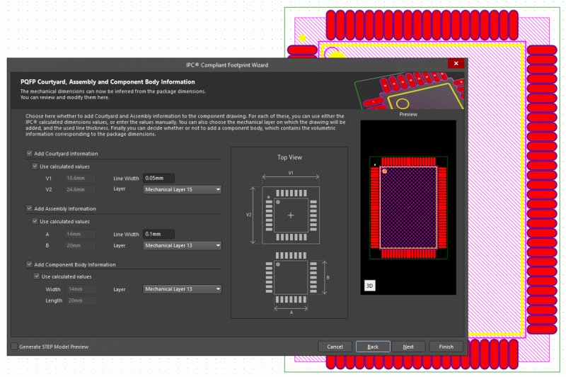
The IPC® Compliant Footprint Wizard dimensions PQFP courtyard
Use MCAD and ECAD to Nail Down Component Dimensions
PCB library models for each part are built from component vendor datasheets. Dimensions are carefully used to build the circuit board component library models for placement during the circuit board layout. Additionally, IPC standards build footprints to enable successful soldering for each conductive lead from the component to the board. Finally, the IPC standard specifies a courtyard that encompasses the entire part and footprint to give printed circuit board layout software enough dedicated room for successful assembly.
- Build your libraries with the footprint, electrical specifications, and pin arrangements.
Component Symbol Information Management and Display Usability
- Make component libraries that port footprints across instantiations.
- Appreciate good libraries with Altium Designer’s IPC Footprint Wizard.
Now that you understand the importance of unified libraries, let’s take a look at Altium Designer’s IPC® Compliant Footprint Wizard in building component models.
Altium Designer IPC® Compliant Footprint Wizard Intelligently Builds Component Models
You’ve chosen your components and you want a powerful way to make compliant footprint models. Altium Designer has the IPC Footprint Wizard to make your work a breeze. The wizard recognizes all IPC-7351 standard footprints and provides elegant menus to easily input dimensions of your part. The wizard includes automatic dimensioning of courtyard, silkscreen, and STEP model.
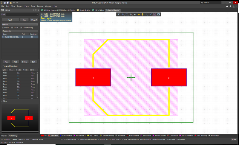
PCB footprint for an SMD electrolytic capacitor
Choose the Best IPC® Compliant Footprint Wizard to Make One Unified PCB Component Library
With Altium Designer’s IPC® Compliant Footprint Wizard, making accurate parts libraries is easy. The models made and stored during schematic capture exist in the same libraries used for PCB layout. You no longer need to keep separate libraries or to keep track of assorted footprint dimensions. Instead, use intelligent tools to build the libraries that result in accurate fabrication and assembly.
- Watch and learn how easy it is to use Altium Designer’s IPC® Compliant Footprint Wizard. See the IPC® Compliant Footprint Wizard in action.
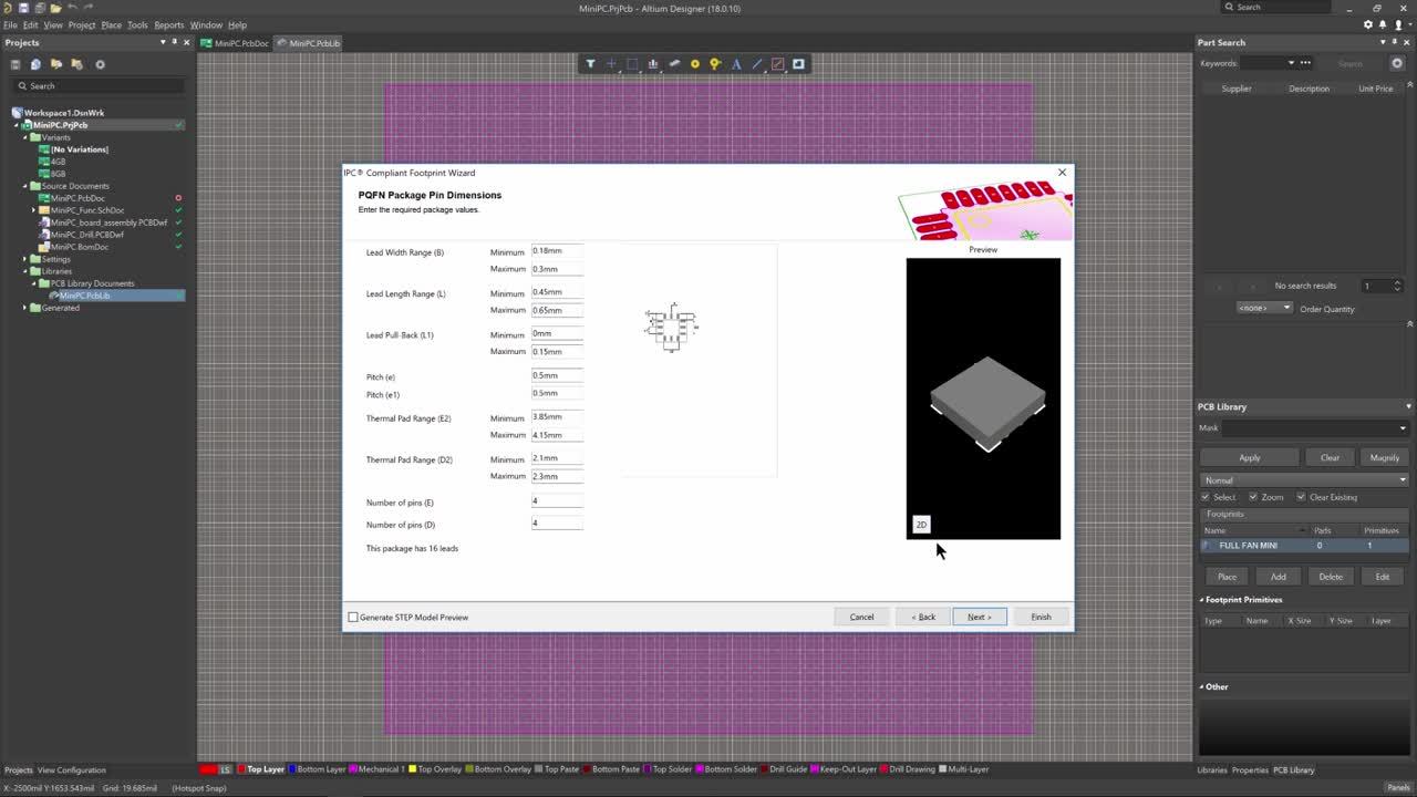
- Consider how to integrate your footprints with MCAD partners. Here are some features to consider during MCAD Integration.
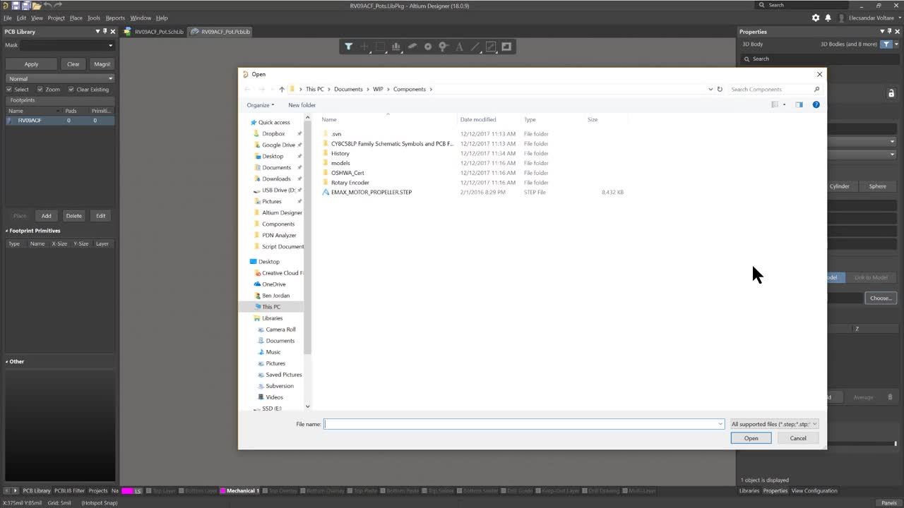
- Incorporate object-specific keepouts to complement footprints. Watch features for object specific keepouts.
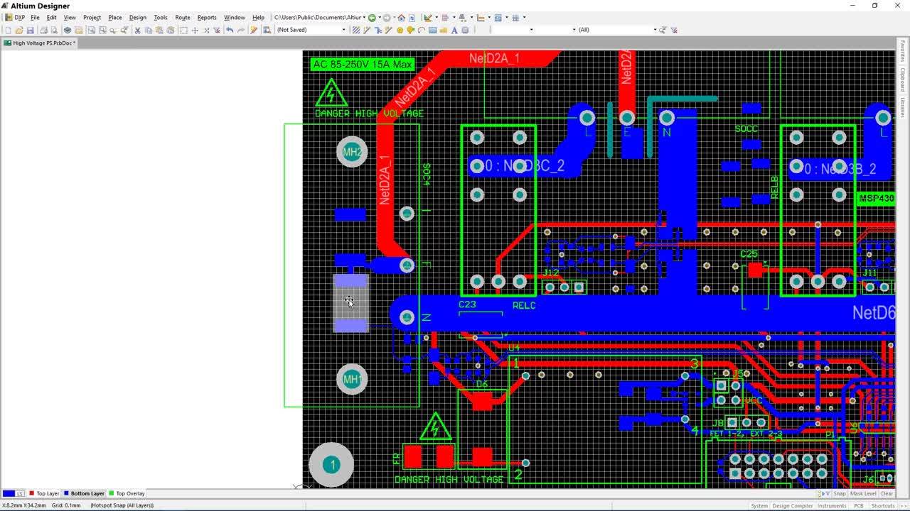
Building component libraries is a vital activity for the preparation of PCB layout, fabrication, and assembly. Component dimensions and models are necessary from the early concept to collaborate with MCAD partners through schematic footprint generation and into PCB layout. PCB layout needs accurate models to correctly represent footprints and landing patterns in Gerbers sent to PCB fabrication. Altium Designer’s unified environment has you covered with STEP models for MCAD to ECAD with the IPC® Compliant Footprint Wizard for your development process from MCAD into PCB layout and manufacturing.


