


The Importance of PCB Documentation


When it comes to real estate, it’s all about location, location, location. When it comes to ensuring a PCB will be built as designed, the emphasis is on documentation, documentation, documentation. This article describes the documents that need to be provided by the board design group to the fabricator, assembler, and test organization. Included is the description of the different drawings needed along with files and notes. All of these documents are of crucial and equal importance. Attempts to circumvent this process and the data contained within can make the difference between a PCB that will successfully operate as designed, or an entire product that is flawed and needs to be scrapped and reinitiated from square one.
How Much Data is Needed in PCB Documentation?
In the final analysis, the PCB design process has three customers as follows:
- The PCB fabricator.
- The PCB assembler.
- The PCB production test organization.
Each of these groups requires data that is extracted from the design database and presented in a form that is usable by the different types of equipment at the three different customers’ facilities. In addition, it’s mandatory to create a document set wherein the design rules and other appurtenant data related to the design of the PCB is contained. The required documents include:
- An engineering drawing on which PCB design data is recorded.
- A PCB fabrication drawing on which the fabrication data is recorded.
- A set of design files that are used to create the film and other fabrication tooling (sometimes referred to as Gerber data).
- A PCB assembly drawing on which assembly information is noted.
- A set of PCB assembly files that includes the bill of material and pick and place information.
- A set of test points that will be used by test engineering to prepare the test fixtures.
The foregoing information is presented in order below.
The Engineering Drawing
The engineering drawing is very similar to the fabrication drawing but contains the design information instead of the fabrication information. This drawing is derived from the outline drawing that defines the size and shape of the PCB. It includes:
- The drill table with drill sizes and estimated quantity and plating info.
- The PCB stackup (which, as noted previously, is one of the most crucial pieces of information necessary for any PCB implementation).
- The list of fabrication notes.
- The technology table that defines the routing rules.
- A list of all the design files that must be prepared for the fabricator.
- The PCB outline drawing.
- A table showing what power supply voltages will be assigned to each power layer. (This is especially important for today’s designs that incorporate a wide range of voltages).
- Other notes as appropriate.
The Fabrication Drawing
The fabrication drawing is derived from the engineering drawing. The final pin count is added to it and the technology table is removed from it. The final PCB L1 artwork is added to the outline drawing and it shows what the finished PCB should look like.
This drawing also contains the PCB stackup and each layer and its name. The design or Gerber data are also listed by layer. A common problem with these two types of information is that the names are not the same between the two files. This leads to layers being incorrectly stacked. Hence, the product developer must use the same labels in the design files as those that are on the stackup drawing.
Figure 1 shows how a fabrication drawing is laid out.
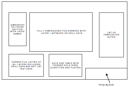
Figure 1. A Typical PCB Fabrication Drawing Layout
Table 1 contains the list of fabrication notes used to build a high-layer, controlled-impedance PCB:
NOTES: (UNLESS OTHERWISE SPECIFIED)
- Reference General Specification for Printed Circuit Boards #_________________
- Any deviation from these instructions must be approved in writing by principal or agent.
- Material: High Tg Fr-4 class laminate with Tg of 170C or higher. All prepreg and laminates minimum two plies, resin content at least 50%, only glass styles 106, 1080, 2113 and 2116 allowed. Board Lamination: Overall thickness:______0.110”±0.010” _____.
- Copper weight: see stackup drawing.
- Drilling: All holes to be located by X & Y coordinates from NC drill data supplied. See separate Drill Table for drilled hole sizes and quantity. Pad stacks are designed for the drilled hole sizes shown. Do not change drill sizes.
- Minimum annular ring of 2 mils on all signal layers, unless otherwise specified.
- Copper plating: Hole wall copper plating to be 0.001” minimum.
- All exposed copper to be plated with electroplated gold over electroplated nickel. 6-10 micro-inches gold over 150-200 micro-inches nickel. (Palladium allowed between nickel and gold)
- Soldermask: Liquid photo-imageable solder mask to be applied over bare copper or gold/nickel plating unless otherwise specified. Color- green.
- Legend/Silkscreen: Use nonconductive yellow or white ink.
- Mark with fabrication revision, supplier ID and date code approximately where shown on bottom or far side.
- All inside corners and slots shall have 0.062 radius ±0.005” or less.
- No modification of film without prior authorization. For exceptions see notes 16 & 21.
- Stripes of copper are plotted on each layer on one side of the PCB edge as shown. These “stacking stripes” are intended to be exposed when the PCB is removed from the panel. Do not remove/modify stacking stripes.
- Compare CAD net list to net list generated from Gerber data prior to fabricating board. Resolve differences prior to building board.
- Non-functional pads to be removed from all inner layers.
- Conductors: Width and Spacing: Build to Gerber data, however, compare widths to Fabrication Drawing Data Set Table and resolve differences prior to fabricating board. GERBER TRACE WIDTHS ARE FINISHED TRACE WIDTHS. Finish width accuracy on inner layers ±0.0005”. Finished width accuracy on outer layers ±0.001.” Fabricator may add manufacturing allowances to trace widths in working film only to accomplish the specified finished trace width.
- This is a controlled cross-section PCB. All fabrication instructions must be complied with in order to assure valid results on completed assemblies. Etch all traces to widths specified in Gerber files. All dielectric thicknesses to be specified ±1 mil. No deviations allowed.
- First delivery to include diazos of film and a copy of the stackup sheet used to select laminates.
- When a socket is mounted on PCB, there is to be selective gold plated on the socket pads to a minimum of 20 microinches.
- Teardrop only on 24 mil and smaller pads at trace exit location. For 24 mil pads, add a 24 mil pad off set from pad center by 2 mils.
- Thieving allowed on outer layers to ensure uniform plating, so long as no thieving lies over the top of traces in the buried signal layer beneath the outer layers.
- Dimensions of dielectric layers and copper thickness to be measured on one PCB of each lot using stacking stripes. Report to be included with first delivery.
- Drilled hole true position relative to CAD data not to exceed 0.005”.
- This PCB has laser drilled blind vias between layer 1 and layer 2. See drill file for details.
Table 1. A Typical List of Fabrication Notes
Table 2 is the list of the design files required to fabricate a multilayer PCB. It also includes the CAD net list, which is designated as the standard, IPC-D-356B .
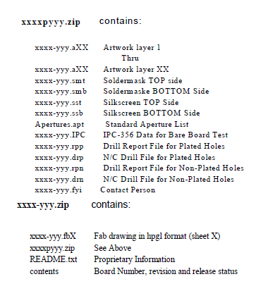
Table 2. List of Design Files Required to Fabricate a Multilayer PCB
This netlist has the location of all the X-Y component pins appended to it. It is used to prepare the bare board test fixture and compares it with the netlist synthesized from the Gerber data.
The PCB Assembly Drawing
The PCB assembly drawing contains the information needed to assemble all the electronic components to the PCB along with the information of how to attach all of the mechanical parts to the board. It should be noted that this list is often several pages long.
Assembly Files
The assembly files contain the X-Y location of all the components; the bill of material; the code to be loaded into the programmable parts and any other information needed by manufacturing operations to assemble the PCB.
Test Point Files
The test point files include the list of test points that are designed into the PCB to provide in-circuit test access to the PCB.
Summary
All of the PCB documentation included as it transitions from the design-to-fabrication, fabrication-to-assembly and assembly-to-production test operations are necessary for ensuring that the PCB will work as designed. This documentation provides the data trail needed to build not only current but future generations of the PCB as well, and the PCB documentation preparation process must be both accurate and complete.
Have more questions? Call an expert at Altium or continue learning about BOM management to keep your PCB design right.
Reference
- Ritchey, Lee W. and Zasio, John J., “Right The First Time, A Practical Handbook on High Speed PCB and System Design,” Volume 1.
About Author
Related Resources
Table of Contents
Design to Release, Without the Friction
- Keep reviews tied to the right version
- Reduce handoff confusion and rework
- Spot sourcing and release risk earlier
- Work solo, share when needed
Get Started
Thank you, you are now subscribed to updates.

