


Optimize Your Multiboard PCB System with Intelligent Design and Manufacturing Solutions

At a Glance
Unify your multiboard PCB workflow with intelligent design tools that align logic, layout, harnesses, and documentation from start to finish.


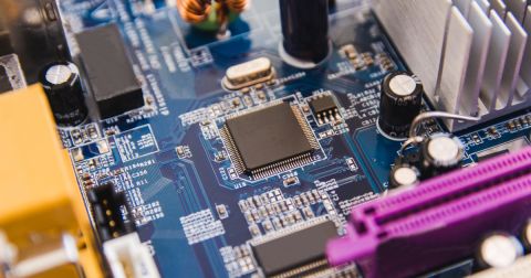
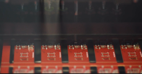
As electronic products continue to become more compact and interconnected, the use of multiple PCBs within a single device has become standard practice. From modular medical equipment to industrial systems and consumer tech, multiboard design architectures allow engineers to optimize layout, improve serviceability and manage complexity through functional partitioning.
Multiboard Design: The System-Level Challenge of Multiple PCBs
But complexity is the tradeoff. Even small misalignments can derail progress. Ensuring physical and logical alignment early is critical to avoiding costly surprises. Yet clarity on questions like “Do the connectors align?” or “Are the inter-board nets mapped correctly?” often arrives too late.
Reducing these risks requires visibility into the entire design, not just individual boards. That means adopting EDA design tools built for system-aware multiboard design from the very start.
What Engineering Teams Need from Modern EDA Tools for Multiboard Design
Engineering teams require digital environments that support system-aware multiboard design across multiple interconnected boards and components. These tools should unify logical connections, physical structure, and layout decisions to create alignment for electrical, mechanical, and manufacturing teams.
Modern EDA tools let engineers define how boards interact, where cables and harnesses are needed and how system components relate. When changes ripple across the system, teams need synchronized tools that adapt instantly, maintaining coherence with the overall system-level design.
For a seamless workflow, traceability and collaboration are critical. This includes enabling engineers with the tools to define interconnect logic, visualize spatial relationships and understand the downstream impact of changes. Mechanical and manufacturing teams also need real-time access to updated 3D PCB assemblies and current design data.
When workflows are fragmented, costly errors can slip through the cracks. Integrated PCB design tools give teams traceability, real-time visibility and a unified view that keeps them aligned from planning through production.
From Concept to Connectivity: A Structured Workflow for Multiboard Design
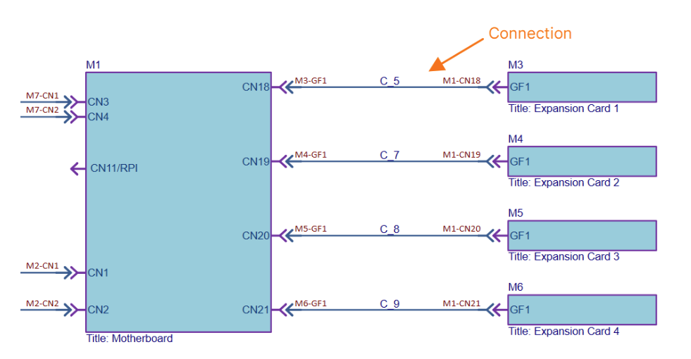
Successful multiboard projects begin with a system-level schematic that maps the complete interconnection strategy and signal architecture. This creates the foundation for strong cross-team alignment in multiboard design.
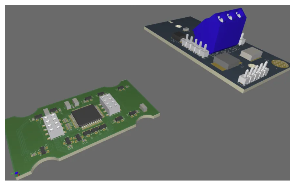
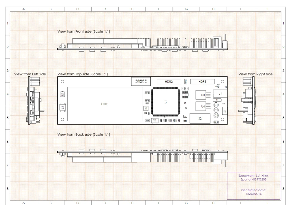
The next step is full-system modeling. Accurate placement and 3D assembly validation help teams avoid misalignment, routing conflicts and enclosure issues before fabrication ever begins.
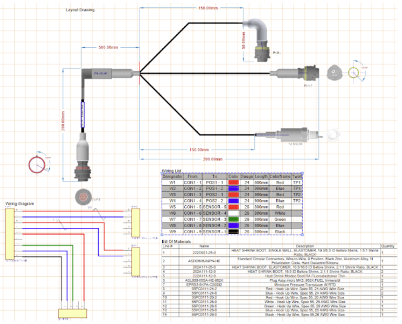
When harnesses are part of the design, documentation becomes critical. Engineers must specify wire lengths, splices, terminals, and labels to meet manufacturing standards. What once were manual steps now become an integral part of the multiboard design process, linking schematic intent to real-world implementation.
Powering Multiboard Design in Altium’s Environment
Altium’s solutions provide an environment built for multiboard coordination. Altium’s unified flow preserves schematic logic all the way into the 3D layout, enabling engineers to align components, validate placement, and verify fit with real-time spatial checks.
At the schematic level, engineers can treat each board as a modular block, with full control over defining interconnects, cables, and harnesses. Net assignments and system structure remain consistent across views so teams understand how the system fits together both electrically and physically.
As the design evolves toward assembly, that logic transitions smoothly into a shared 3D space. Boards are positioned, aligned, and validated with spatial checks that help prevent physical interference and ensure correct enclosure fit. This gives visibility into how subassemblies interact and helps avoid surprises downstream.
Streamlining Integration with Harness Design in Multiboard Systems and Collaboration
With Altium, harness design bridges schematic intent and physical implementation. As Krishna Sundaram, Senior Product Manager at Altium, explains: “You can represent splices, lengths, terminals, labels – everything needed to communicate with your contract manufacturer.”
3D modeling and collaboration tools further streamline the integration process. Engineers can visualize harness paths, adjust board placement, and verify fit before committing to a physical build. “You can automatically see every net name translated from the multiboard schematic to the wiring diagram, so you know exactly which pin connects to which,” Sundaram adds. Wire lengths, pulled directly from mechanical data, deliver consistency between design and enclosure.
With shared access, inline commenting, and task tracking, Altium solutions help teams stay in sync, accelerate reviews, and reduce feedback loops. This keeps the product development process moving forward without interruption.
System-Level Testing and Validation in Multiboard System Design
Before a multiboard system reaches production, testing must confirm that each board works both independently and as part of the complete system. Altium solutions support system-level DRC rule checking, signal integrity analysis, and simulation tools that help identify errors early. By integrating test planning into the design environment, teams can ensure that no assumptions go untested and avoid late-stage iteration cycles.
In addition to standard DRCs, Altium provides system-level rule checking and continuity validation across boards and harness interfaces. Engineers can simulate signal behavior across connector boundaries, validate impedance continuity through harness paths, and assess cross-board interactions using system-aware layout diagnostics. These tools enable earlier intervention and help ensure functional integrity before the first prototype is built.
Reliable Outputs for a Smoother Path to Production in Multiboard Design
A successful handoff depends on outputs that reflect the entire, current system. Inaccurate files or outdated documentation introduce delays, costly errors, and quality risks. Altium solutions keep manufacturing data synchronized with the latest design state, helping teams move into production smoothly.
Draftsman tools support section views, detailed callouts, and full assembly overviews that automatically update as designs evolve. Output packages — including 3D assemblies, structured harness diagrams, and dynamic BOMs — ensure manufacturers have what they need, when they need it, with fewer handoff errors.
Design Once, Deploy Across Platforms in Multiboard Design
Many organizations build product families around shared architecture. Altium simplifies multiboard design reuse: engineers create modular assemblies, reuse validated layouts, and apply consistent design rules across multiple products. This accelerates development cycles and helps maintain quality—whether for a derivative or a completely new generation.
Altium’s multiboard environment supports version‑aware modules that retain schematic logic, placement integrity, and harness definitions while adapting to new constraints. Engineers can override design elements per variant without fragmenting the base architecture. This flexibility supports tiered product lines and market-specific adaptations while preserving the core system design.
Compliance‑Ready Documentation Built Into Multiboard Design
Multiboard systems used in regulated industries must meet stringent compliance requirements, including traceable design records and validated manufacturing outputs. Altium’s integrated documentation tools help teams generate the full suite of compliance files, from labeled harness schematics to verified material declarations. This reduces audit risk and simplifies certification processes in compliance-ready multiboard systems.
Features like automatic part traceability, revision-controlled outputs, and embedded compliance notes help guarantee documentation matches the live design state. Teams can embed RoHS, REACH, or UL data into BOM outputs, generate IPC‑compliant harness diagrams (e.g. IPC/WHMA‑A‑620E), and produce assembly reports tailored to regulatory formats. With all compliance materials originating from the design source, engineers eliminate transcription errors and reduce dependency on third-party validation systems.
Building Confidence into Every Stage of Design
When teams align from the start, they deliver faster with fewer surprises along the way. Altium empowers engineers to connect planning, layout, and output in one intelligent workflow. From system schematics to harness routing and board placement to production documentation, engineers gain the clarity and coordination needed to deliver multiboard PCB systems with precision.

About Author
Related Resources
Related Technical Documentation
Table of Contents
- The System-Level Challenge: Designing with Multiple Boards
- What Engineering Teams Need From Today’s EDA Tools
- From Concept to Connectivity: A Structured Workflow
- Powering Multiboard Design in Altium’s Environment
- Streamlining Integration with Harness Design and Collaboration
- System-Level Testing and Validation
- Reliable Outputs for a Smoother Path to Production
- Design Once, Deploy Across Platforms
- Compliance-Ready Documentation Built In
- Building Confidence into Every Stage of Design
Design to Release, Without the Friction
- Keep reviews tied to the right version
- Reduce handoff confusion and rework
- Spot sourcing and release risk earlier
- Work solo, share when needed
Get Started
Thank you, you are now subscribed to updates.