PCB Design Tips for EMI and SI Part 1

In this two-part series of articles, we are going to be looking at the basic principles and ways you should route and lay out your PCBs to minimise chances of EMI problems and to maintain proper signal integrity.
This first article outlines the basics of signals, energy, and fields, as well as rise and fall times in the digital domain and what this means for us as PCB designers.
Signals, Energy, and Fields
The core takeaway and what a large number of people don't realise when it comes to electronics and PCB design is that the electric and magnetic fields contain all of a signal’s energy.
Most people think energy travels in the copper, for example, the signal trace or return plane - but in fact it does not! The signal energy contained in the fields travels in the dielectric space between the trace, which constitutes the forward path, and an appropriate copper plane below the trace, which constitutes the return path.
The forward and return paths so the planes or traces must be well defined at all times to main proper signal integrity and EMI. In essence, one can think of the copper acting simply as a waveguide for the fields.
Microstrip and Stripline
Microstrip (Source: Rick Hartley)
Stripline (Source: Rick Hartley)
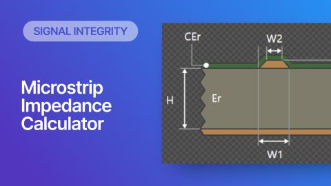
Here is a simple illustration of the electric and magnetic fields in a PCB, as seen for microstrip and strip-line. For a microstrip trace, an outer-layer trace which isn’t buried in dielectric material, we have essentially air as our first dielectric and then the dielectric of the PCB underneath. There's quite a lot of fields spread for both the electric field, which is in blue and the magnetic fields, which are shown in red.
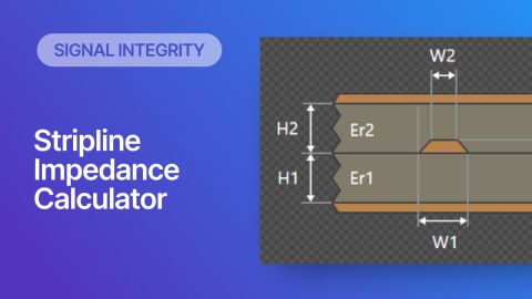
Alternatively, on the right-side image, the strip-line trace shows that the fields are better contained, because we have reference planes at the top and below the trace in the middle. Simply speaking, the electromagnetic fields like to attach to these return or reference planes – and for strip-line traces, are now better contained.
Thinking about electric and magnetic fields like this, rather than electron flow in copper, is the key when designing PCBs with respect to EMI and SI, and containing fields. Proper EMI and SI performance is basically what this is all about.
Frequency in the Digital Domain
Another misconception is when it comes to frequencies in the digital domain. For example, many people assume that the highest clock frequency of a signal (for example, of a microcontroller) in a design, is the highest frequency of concern in that system. This couldn't be further from the truth!
Typically, these days we are in the digital domain where we rely on square waves to transmit data. Of course, these square waves won't be ideal – they’ll be closer to trapezoids, as we have finite edge rates (rise and fall times). The fundamental period of these square waves might be our clock frequency, for example, a microcontroller’s 8 or 16 MHz clock signal. The catch is that we don't need to just be concerned with this fundamental clock period - we also need to be concerned with the edge transitions!
These edges are where the bulk of the signal energy and the frequency content is contained - rather than the fundamental clock period. The highest frequency of concern, given these rising and fallen edges, can be determined by the Fourier series of a square wave, for example.
Typically, we don't go to that much effort, and we can derive a simple approximation to give us the signal bandwidth in GHz, given a rise/fall time (10% to 90%) in ns:
fmax=0.5t(rise/fall,ns)GHz
We use either the rise or the fall time depending on which is the fastest.
Finding Rise and Fall Times
That's a great and simple approximation - but the question is how do we even figure out an IC’s rise and fall times? Usually from data sheets this information isn’t entirely evident. If rise and fall times are listed, they are typically given as the best case (which corresponds to slowest rise and fall times). However, they’re not giving us the minimums, which in turn lead to very high bandwidths.
We should in any case strive to design for the worst case – so we need to dig deeper to find these rise and fall times.
Luckily, most manufacturers provide IBIS files for their ICs. IBIS files are typically used for simulations, and we can extract rise and fall times from them as well. Once you have the IBIS file downloaded from your IC manufacturer’s website, open it, and look for the RAMP section.
The RAMP section states two parameters: dv/dtr and dv/dtf. You might’ve guessed already that these stand for the rise and fall rates (voltage change per time change), respectively. We need to be careful, however, as the IBIS models specify rise and fall times from 20% to 80%, whereas our definition to find a signal’s bandwidth uses 10% to 90% rise and fall times!
Keep in mind these numbers are also for specific loading (typically for a 50 Ohm load connected and your system of course may be different).
For an ATMEGA328P (a very common microcontroller), the worst-case rise/fall time was given in the IBIS file as 0.76ns. Converting this from a 20%-80% to a 10%-90% value by linear scaling (approximately, multiplying by 1.3), we arrive at a rise/fall time of just over 1ns.
What Does This Mean?
Plugging this value into our bandwidth approximation formula, we arrive at a bandwidth of 500MHz!
Pretty astounding, given the fact that we initially thought we’re working with a ‘slow’ microcontroller in the 10s of MHz range. All of the frequency content is hidden (so to speak) in these rising and falling edges.
Following on from this, it turns out that we need to take care (think: controlled impedance, reflections, etc.) when our trace lengths start to look like distributed elements rather than lumped elements. This means that the trace length starts to be comparable to the wavelength of the highest frequency component.
At 32MHz this would be at around 25cm for a microstrip trace. However, at 500Mhz we need to take care at a trace length as short as 17mm!
In addition, fast edges typically give rise to more emissions – thus being more prone to causing EMI problems than signals with longer rise and fall times.
Containing fields and identifying signals with fast edges – and then controlling their traces - are the basics elements and key aspects to designing PCBs successfully with regard to EMI and SI.
In the next article of this series, we’ll examine PCB design techniques that help us achieve field containment and control of fast-edge-rate signals.


