PCB Design Tips for EMI and SI Part 2

In this two-part series of articles, we are going to be looking at the basic principles and ways you should route and lay out your PCBs to minimise chances of EMI problems, and to maintain proper signal integrity.
The first and previous article outlined the basics of signals, energy, and fields, as well as rise and fall times in the digital domain, and what this means for us as PCB designers.
This article illustrates a few essential PCB design techniques to control fields, and to deal with fast-edge-rate signals—the fundamentals of EMI and SI, so to speak.
Field Containment
Before we get to specifics, let's briefly talk about how we control EMI and SI from the information we discussed in the previous article. We outlined the basic idea that energy is stored in the fields between the dielectric (the “dielectric space”). Our main job as PCB design engineer, is to control and channel that energy and those fields.
One of the most important parts of field containment and controlling EMI is the stack-up (for a more detailed discussion on PCB stack-up and build-up, make sure to check out this video. Firstly, it’s advisable to use thin dielectrics between signal and reference planes. This improves the coupling between forward and return path, reduces inductances due to small loop areas, and if we have power and ground planes adjacent with thin dielectric, this of course increases the interplanar capacitance. In return, this also improves power delivery.
Suggested 4-Layer Stack-Up for Routed Power
Keep in mind that closely spaced layers decrease the trace width for a given impedance, and therefore will be more prone to manufacturing tolerances. The available materials and producible stack-ups will depend on your PCB manufacturer of choice.
Not only do we want to have closely spaced layers for field containment but also always a ground (or suitable reference) adjacent to every signal and power plane. If we have two adjacent signal layers, the fields will interfere leading to poor SI. If we have a signal layer without a directly adjacent return plane, the fields will spread, leading to poor EMI performance.
Critical Trace Length
With regards to traces, we want to keep them as short as possible to make sure that the traces are seen as lumped rather than distributed elements. Distributed elements require proper impedance control and termination. Ignoring this will lead to poor EMI and SI.
The question is, how long do traces have to be (for a given maximum frequency) to appear as distributed elements (termed “critical length”)?
The general formula is shown below, where c is the speed of light, ε the effective dielectric constant, and f our maximum frequency of interest:
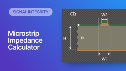
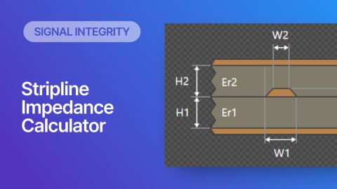
In effect, it is the wavelength within the dielectric material divided by twenty. As usual, the length changes depending on if the trace is routed as a microstrip (outer layer) or stripline (inner layer). This is because waves propagate at different speeds in different dielectric materials.
As an example, for a 1G Hz signal, the critical length is 8.3 mm for a typical microstrip trace.
Above these lengths, the traces themselves (or rather the transmission lines) behave as distributed elements. Once traces behave as distributed elements, we need to control their impedance as they are not “invisible” anymore to the driver and receiver.
Transfer Vias
Another tip to improve EMI performance in your PCBs is the placement of transfer vias.
When switching layers with a signal via, we typically also change reference planes (think of a four-layer SIG-GND-GND-SIG board, for example). While we are still routing on the top layer with a trace, for AC signals (>20 kHz), the return path is directly in the reference plane below. Once we are on the bottom layer, the return path is in the reference plane above.
However, what happens to the return path and thus the fields when we move along the via in the Z-axis when changing layers? Then fields will spread as they try to find a suitable “attachment point” (a return path), which can be a cause of EMI problems.
In this case, we want to place a transfer via—which is basically a grounded via—close to the signal via. This is to maintain a defined reference and return path while transitioning along the Z. Note that this transfer via only works if the references we are switching between are both the same type (for example, GND to GND).
If we’re switching from a GND to PWR reference, we need to place a small-valued capacitor stitched between GND and PWR reference close to the transition point.
Splits in Reference Planes
Most PCB designs shouldn’t require any splits in (GND) reference planes. If they do, these splits need to be carefully designed, as well as any traces routing near them.
Traces should under no circumstances cross a split in a reference plane. We constantly need to remind ourselves of where the return path is, and what the fields would do, should we cross a split in a reference plane.
Unintentional splits in reference planes can occur due to via anti-pads voiding the plane. It is therefore preferential—if space allows—to space vias and holes far enough apart to not cause large splits in the reference planes.
Reducing Rise/Fall Times
A further aspect is to choose ICs that can do the job we need them to do with the slowest rise and fall times possible. Slower rise and fall times mean less energy and thus a reduced signal bandwidth.
If choosing a different IC is not an option, we can decrease the bandwidth (rise/fall time) of a signal by placing a series of resistors at the output of a transmitter. Resistors in combination with the capacitance seen on the line forms a low-pass filter. Depending on required data rates, you may also want to place a small capacitor on the line as well—be cautious when doing this though.
This two-part series gave a brief overview of PCB design issues that can cause EMI and SI issues. The tips illustrated in this brief guide, along with powerful PCB design tools such as Altium Designer, can help mitigate EMI and SI problems during the design process.


