


DDR5 vs. DDR6: Here's What to Expect in RAM Modules

At a Glance
What can designers expect in DDR5 vs DDR6 RAM? Here’s what you can expect for your next memory device.


While DDR5 was still being finalized, DDR6 was just being discussed, even as designers who were already comfortable with DDR4 were grappling with a new version of this classic RAM technology. Fast forward to today, and DDR5 RAM sticks have just hit the market, and meanwhile the biggest names in semiconductors are working on DDR6. Designers working in the ultra-fast domain will be taking clock and data speeds to new levels to get even more data out of their memories.
The move from earlier DDR generations into DDR5 and DDR6 brings new packaging, new clock and error correction codes added to bitstreams, and of course a higher data transfer rate. So what else can designers expect from DDR6 RAM? Let’s look at a comparison of these two technologies as a comparison will help the avid computer peripherals designer prepare to use both.
From DDR1 to DDR5 and Beyond
DDR is one of the few technologies that remains primarily a parallel bus with a mix of single-ended and differential signals. From the original DDR specs up to DDR5 and DDR6, the routing topology and capabilities of these systems have evolved significantly over time. The table below compares some of the critical specs of DDR technologies up to the current DDR5 spec and the expected capabilities in the DDR6 spec.
|
|
|
|
|
|
|
|
|
|
|
|
|
|
|
|
|
|
|
|
|
|
|
|
|
|
|
|
The above table shows that the continuous doubling in the base standard is also used in DDR5 and DDR6. The JEDEC standard expects DDR technology to scale up to 8 GHz by 2024. For perspective, take a look at the speeds in commercially available RAM modules (and related GDDR modules) shown in the graph below (graphic provided by Keysight).

Up to DDR3 and DDR4, designers needed to be worried about designing to controlled impedance, maintaining length matching, and preventing crosstalk within the bus. Once you hit DDR4 and higher, problems like dispersion, jitter, and copper roughness start to contribute more to signal integrity as bandwidths get pushed farther into the GHz levels. DDR5 pushes this even further, but it changes the topology somewhat and adds in new capabilities for error correction and signal recovery at the receiver.
DDR5 and DDR6 Topology
DDR5 and DDR6 take the top-end DDR4 data rate and double it again (and another doubling in DDR6) by making buses faster, rather than wider. You’re still dealing with DDR4 routing challenges in terms of laying out parallel single-ended nets, but these channels are much shorter. Buses will also run fast enough that typical channels will usually be electrically long, so bit errors will be dominated by insertion losses along interconnects.
Some points in the DDR5 and DDR6 standards have not changed from DDR4:
- Error correction code is maintained
- Total bus width is 64-bits
- Flyby topology is still used in routing
The major change in DDR5 and DDR6 is the splitting of the bus from a single 64-bit channel into two 32-bit channels. These two channels each have their own error correction codes (8 bits) applied separately to each channel. This makes the equivalent bus width wider when the error correction codes are included in the bus.
An example DDR5 RAM module provided by Rambus is shown below. This exmaple splits the channels off on each side of the registered clock driver (RCD) chip, which provides clock distribution to each DRAM module. Splitting the channels in this way requires splitting the differential clock out to two channels as well. The reason cited for doing this is to aid signal integrity in each channel. DDR6 follows the same approach, but with 4 channels at 16 bits each instead of 2 channels.

Finally, RAM modules will have their own power regulation applied directly on the module, rather than relying on power regulation from the main board. Bringing a regulator onto the module provides isolation from the main power rail through rectification in the regulator circuit. This is beneficial because other components will be pulling from the main power rail, and their ripple could telegraph over to the module despite applied decoupling. The regulator provides some natural isolation and allows the decoupling strategy (decaps and stackup design) to be moved to the module.
DDR5 and DDR6 Equalization
To address the insertion loss issue I mention above, DDR5 and DDR6 both adopt decision feedback equalization (DFE) to aid signal recovery at the receiver. This technique helps open the eye on a bitstream so that signal levels can be clearly interpreted when they are received. This is a standard approach to addressing signal recovery in insertion loss-dominated channels when bandwidths begin to stretch to very high frequencies.
The need for equalization arises due to the signal bandwidths in DDR5 and DDR6. Both standards require chips that push bandwidths on edge transitions so high that effects like roughness and dispersion become excessive. The signal level is also lower in DDR5 and DDR6 compared to earlier generations. The result is excessive attenuation at high frequencies and closure of the eye in a bitstream. DFE is one equalization technique that helps open the eye so that signal levels in a bitstream can be distinguished. It is also used in the newest standards revisions of other high-speed protocols.
PCB Design Challenges in DDR5 vs. DDR6 RAM
The challenges in DDR6 RAM occur largely at the chip level, but the same board-level challenges in DDR5 also apply to DDR6 RAM. The power integrity challenge in DDR5 I mentioned above isn’t going to go away in DDR6 RAM. The power integrity challenge with DDR6 is extending flat PDN impedance out to higher signal bandwidths once modulation is imposed on DDR6 signals. Extending flat PDN impedance out to higher frequencies is all about keeping jitter at the Tx side low, which then keeps ISI at the Rx side low enough so that signals can be resolved with equalization. On-board power management ICs for DDR5 modules will also appear on DDR6 RAM modules to help regulate power throughout the module.
There are plenty of other design challenges to consider in DDR5 and DDR6, but those listed above are arguably the greatest. You can read more about DDR5 PCB design challenges in an earlier article. DDR6 isn't even commercially available, and yet there are already projections on performance for DDR7. One of the major applications of that memory architecture could be 8K gaming, VR/AR, and any other immersive experience relying on ultra-high quality video.
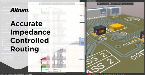
When new technologies like DDR5 vs. DDR6 RAM come along, you need the design features in Altium if you want to lead technology development. Altium includes a set of powerful layout and routing features that are ideal for high-speed applications.

About Author
Related Resources
Related Technical Documentation
Table of Contents
Design to Release, Without the Friction
- Keep reviews tied to the right version
- Reduce handoff confusion and rework
- Spot sourcing and release risk earlier
- Work solo, share when needed
Get Started
Thank you, you are now subscribed to updates.

