What is an Eye Diagram?

There are many ways to characterize high speed digital channels, with the goal being to verify specific signal integrity metrics that illustrate channel compliance. Things like S-parameters and impedance are useful, but there is one important measurement to be evaluated with a digital bitstream: an eye diagram.
The eye diagram is a useful measurement or simulation as part of channel compliance. The measurement shows many different factors that can affect signal behavior simultaneously, ultimately allowing for qualification of errors and losses in a channel. In this article, I’ll run over some of the fundamental measurements that you could manually extract from an eye diagram and how they reveal some strategies for improving channel designs.
Eye Diagrams in Signal Integrity Analysis
What is an Eye Diagram?
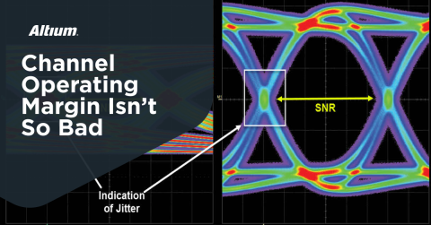
One of the fundamental measurements used to qualify channel designs in digital systems is an eye diagram. This involves superimposing rising and falling edges of a bitstream in a time domain sampling trace, such as with an oscilloscope. A signal integrity simulator can perform the same type of superposition of signal levels. By overlaying the rising and falling edges, it’s easy to visualize the level of variance in signal behavior.
Variances that can lead to bit error rates are the main quantities to be determined from this measurement. With overlaid signal traces, it’s possible to take statistics at various points along the time domain measurements. The image below shows an example eye diagram and a histogram of measurements taken from the LOW signal level in the trace. From this histogram you could fit the data to a normal distribution using calculations of the sample standard deviation and the average signal level. The resulting normal distribution is overlaid on the data below.

What You Can Learn From an Eye Diagram
This diagram helps you quantify a wealth of information from a single measurement. You can extract the following information directly from an eye diagram measurement:
- Timing jitter: The variation in rise/fall initiation can be seen directly from an eye diagram when you look at the signal crossings during switching. This would account for both random noise and timing skew in a differential pair.
- Signal level variance: You’ll be able to easily see how the signal level varies. This is, in general, some function of the timing jitter plus other random noise. Signal levels can also vary depending on impedance mismatches.
- Average rise/fall time: This is equal to the time between the average 90% signal level time and the average 10% signal level time. It is related to both the channel response and noise in the system. If there is strong reflection, noise, or ISI, the rise/fall times may not be smooth and could exhibit plateaus or strong variance.
- Average symbol duration: This is the time between the midpoints of consecutive signal crossings.
- Bit error rate (BER): By comparing logic thresholds with the received bits in the eye diagram, it’s possible to determine a bit error rate. This value will depend on several factors, but a desirable value can be as small as 10-12 or lower. Techniques like equalization and pre-emphasis are two ways to decrease BER values. For example, dynamic feedback equalization (DFE) is used for 400G with PAM-4.
Intersymbol Interference
The condition where successive signals interfere with each other due to signal integrity problems is intersymbol interference. By examining intersymbol interference resulting from successive bits, it’s possible to identify specific problems in a digital channel. The ISI you find in a channel is a summative metric, Jason Ellison provides a good overview and comparison with insertion loss deviation in this article.
This raises a converse question: what would constitute an objectively desirable eye diagram? Ideally, you would have zero signal distortion, zero jitter, zero pulse spreading, and zero amplitude noise. In other words, the output signals exactly match the input signals. The ability to see this is what makes eye diagrams such a fundamental part of signal integrity!
How to Read an Eye Diagram
The eye diagram you generate for a high-speed channel illustrates the statistics of signal transitions between different level and the statistics for voltages at each logic level. This gives you a measure of noise that exists at the receiver due to intersymbol interence, crosstalk, and any phenomenological noise added to the channel (level jitter on the driver's I/O power rail). However, the typical metric used to read an eye diagram is its mask, or eye opening.
The eye opening looks at the region in the interior of the eye diagram. To see the eye opening, we can look at the following example for a 224 Gbps PAM-4 channel. The below simulation shows an eye diagram for a pseudorandom bitstream for a ~700 mil long channel between a chip and its connector module; this was calculated with Simberian. When the only jitter that is present comes from reflection at a perfectly terminated load up to the required 56 GHz channel bandwidth, we see that the eye opening is very clear with ~220 mV separation between signals.

We can see clearly that the eye opening along the time axis ranges from about 44% to 57% of the unit interval (UI). This illustrates the amount of jitter seen at the receiver only due to incoming pulses interfering with reflected pulses. The range of the jitter in this channel is about 1.16 ps of variation only due to the superposition of pulses.
Once random jitter is added to the channel, we see some blurring of the eye pattern as the crossing points begin to vary on the time and voltage axes. The below result shows what happens when just 5% random jitter (st. deviation in UI) exists on the rising edges of signals being driven into the channel. This level of jitter might seem small, but given the ~9 ps UI value and 25% UI rise time this is enough to shift level crossings significantly. The result is that the vertical distance between levels and reduced horizontal distance between crossing points.

The moral of the story is: jitter can be seen as a source of noise in the time domain that increases the level of noise in the voltage domain, and this change in the level of noise can be seen in an eye diagram. In another article, I'll look at the interplay between random jitter eye opening so we can see an acceptable limit on random jitter that can be tolerated in a channel.
Measuring and Simulating Eye Diagrams and BER
As I mentioned earlier, eye diagrams can be simulated, either from a channel model with known S-parameters/transfer function and defined buffers, or directly from a PCB layout with all parasitics present. If channel models are known, an eye diagram can be simulated from a pseudorandom bit sequence with a convolution operation (see the block diagram below). This process could be implemented in Matlab or another mathematical scripting program.

When working with a prototype, ultimately the goal is to determine compliance and extract a channel model from measurements. The channel model will be very useful for further design tasks, such as if you were to add a connector or via transition. Determining channel compliance will also require analyzing BER, which can be quite involved and I won’t run over all avenues here. To learn more about analyzing eye diagrams, take a look at this article from Tektronix. In addition, there are other measurements you can extract from your eye diagram; take a look at this support article from Keysight for guidance on other measurements.
When you need to place components, route transmission lines, and access powerful simulators for your digital system, use the complete set of PCB design tools in Altium Develop. When you’ve finished your design, and you want to release files to your manufacturer, Altium Develop makes it easy to collaborate and share your projects.
Whether you need to build reliable power electronics or advanced digital systems, Altium Develop unites every discipline into one collaborative force. Free from silos. Free from limits. It’s where engineers, designers, and innovators work as one to co-create without constraints. Experience Altium Develop today!


