Learn How to Design PCBs with the Best PCB Design Tutorial

Let’s face it: PCB design is complex, and not all design software packages have the tools to help you be successful. Whether you’re creating a simple two-layer board or a complex high-speed digital system, Altium Designer has the design tools and PCB design tutorial you need to get started and succeed. You’ll have access to multiple PCB design tutorials to help you gain a better understanding of advanced features as you venture deeper into PCB design.
ALTIUM DESIGNER
An easy-to-use tool that guides you through successively more advanced PCB designer tasks.
If you’ve ever used a new piece of software, you know about the learning curve involved. With so many different PCB design packages on the market, getting up to speed quickly requires design software that places all of your critical design tools in a single interface. Why not purchase PCB design software that shows you how to be successful? Other design software platforms claim to integrate features, but they still separate critical design tools into addons without providing the guidance new users need to be successful. Instead, you should use design software that gathers all your design tools in one place alongside design resources.
Altium Designer is your answer. Forget about learning through trial and error, your PCB design software should guide you through the basic design tools and introduce you to advanced features that maximize productivity. Add to that a vibrant design community, extensive knowledge base, design webinars, blogs written by experts, and an extensive PCB design tutorial, and Altium Designer helps set you on the path to success.
PCB Layout Basics Part 1: Getting Started with Circuit Board Design Software
Learning how to design a PCB layout can be separated into two major tasks. Before you create a layout, you need to create a schematic that includes the components your system needs and shows connections between them. Once your schematic is created and successfully verified, you can transfer your design to a PCB layout, which defines the physical architecture of your board. This may seem simple enough, but each task requires several interdependent steps. Moreover, there are constraints and guidelines that must be followed to ensure your design can actually be manufactured.
Managing this process is daunting, but a circuit board design application like Altium Designer can help guide you through the process. When you know what to look for in your layout, you can spot when you’ve made mistakes and can quickly correct them before you finish your circuit board. Rest assured, Altium’s rules-driven design engine is designed to help you be successful.
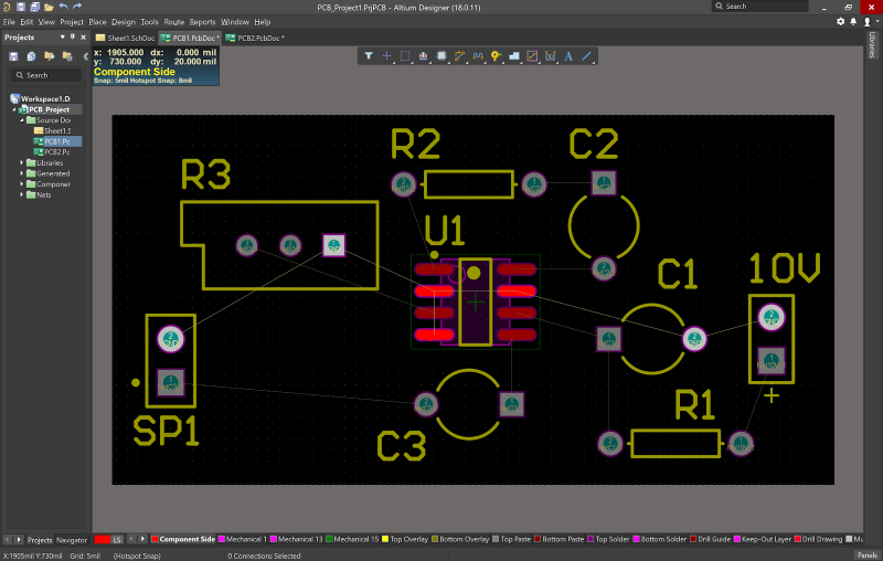
The PCB layout tutorial environment in Altium Designer can be as simple as you need.
Altium Helps You Beat the Learning Curve
Who has time to learn PCB design through trial and error? Whether you are about to design your first printed circuit board or you have years of successful design experience, your new PCB design tutorial for beginners package should help guide you through the design process. The rules-driven design engine in Altium Designer is a critical portion of the application. You’ll be able to quickly see the following list of design errors and advice on how to correct them when you’re designing a circuit board layout. Here are some of the important design mistakes you can catch in your PCB layout:
- Clearance violations: Clearances are important parts of electrical functionality and manufacturability. You’ll need to maintain strict clearances to ensure consistent trace impedance, prevent ESD, component spacing, and much more.
- Silkscreen solder mask errors: Solder mask openings and silkscreen are important for assembly, and your design software should show you any conflicts related to your silkscreen and solder mask placement.
- Cross-probing: The ability to select an error and be pointed directly to a spot in your schematic or PCB layout helps you see exactly what needs to change as you build your design.
Altium gives you more than just design tools. If you need a PCB design tutorial to help you get up to speed quickly, you’ll have access to a variety of resources you need to be successful. The resources listed below contain PCB routing tutorials, guides on how to use PCB design tools, and much more. Anyone can access Altium’s knowledge base, blogs, webinars, and more for free.
- You can get a great introduction to each feature in Altium Designer. Altium gives you access to video Altium Designer tutorials for each design feature. Learn how to design a PCB layout with Altium Designer’s feature tutorials.
- Altium provides you with access to live and on-demand webinars. Experts in the field will be there to introduce you to the new layout, routing, and electronic component integration techniques. Learn more about Altium’s PCB layout tutorials and webinars.
- Altium’s intuitive user interface makes it easy to get started, even if you’re new to printed circuit board design. Behind this simple interface lies extreme design power. Learn more about Altium’s easy-to-use design interface.

Altium Designer guides you through your first schematic and helps you learn how to design a PCB layout.
PCB Layout Basics Part 2: Break Out of the Design Rut With Comprehensive Resources
It’s easy enough to create schematic symbols and PCB footprints with Altium Designer, but everyone needs resources to stay inspired and overcome design challenges. Circuit board parts have been traditionally difficult to find, and many designers have spent hours creating these parts manually. Altium Designer offers access to a Manufacturer Part Search panel, which helps you quickly add components to your library. All you have to do is search and click to download accurate parts directly from a managed library.
When you need more resources to finish a complex design, Altium gives you free access to PCB design tutorials (both online and in-application) that guide you through the various design features. Altium also gives everyone access to their knowledge base through their website. The technical documentation for Altium Designer includes many thoroughly explained examples to help you use design tools. Simply search the knowledge base for a function in the program, and you’ll have instant access to complete tool information and PCB design tutorials.
Once you have your new circuit board layout finished, it’s time to prepare your board for PCB assembly. If it’s your first time creating manufacturing outputs, your design software should be just like a PCB layout tutorial: easy and intuitive. Here’s how Altium Designer helps you quickly generate manufacturing documentation.
Creating Manufacturing Outputs with Altium Designer
The most important thing you can do to ensure a smooth PCB manufacturing process and PCB assembly is to follow your manufacturer’s DFM guidelines. Contrary to what some believe, DFM is specific to your manufacturer. Reliance on default or general specifications can cause manufacturing delays and may require design changes. This is easily avoided by setting up your DRCs to match the capabilities of your manufacturer.
After checking your layout against your design rules, you can generate manufacturing output documentation for your fabricator. This includes Gerber files, pick-and-place files, assembly drawings, and much more. A great way to assist your manufacturer is with panelization. Altium makes panelization easy, including the ability to evaluate 3-D views to determine the best panel arrangement.
- The rules-driven design interface in Altium Designer is central to ensuring functionality and manufacturability. Setting up design rules at the beginning of a project is extremely easy with Altium Designer.
Learn how to ensure manufacturability by applying DFM with Altium Designer.
- The BOM generation tools import real-time component data to ensure component availability. Altium Designer’s intuitive interface makes it easy to prevent manufacturing errors.
- Panelization helps you manufacture at scale and reduce costs. Altium Designer makes panelization quick and easy.
Learn more about circuit board panelization in Altium Designer.
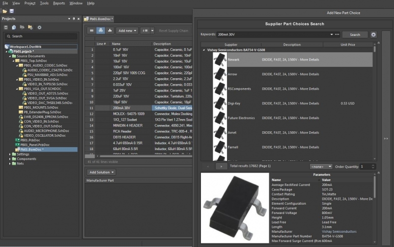
Real-time circuit board component data for your BOM and PCB assembly
PCB Layout Basics Part 3: Rules-Based Design Capabilities Help You Stay on Track
Working in a unified design environment gives you access to all the features you need to get started designing your next PCB. Altium Designer uses a rules-based design that helps you avoid simple mistakes. If you’re new to PCB design or you’re new to Altium Designer, the intuitive interface allows you to start designing schematics from the moment the program starts. Capturing your schematic in your layout is simple, allowing you to start routing connections between components and finish building your new device. All along, the rules-driven design engine, PCB design tutorial, and online resources will help you stay on track.
Altium Designer Makes Design Rules Work for You
Once you’ve determined your device requirements for your application, Altium Designer allows you to encode these specifications in design rules. The design environment in Altium Designer is fully customizable. You can rest assured your layout will comply with your design rules, and you can check and correct any rules violations quickly and easily. These rule definition and checking features help you stay within standard design guidelines and help you build a device that meets your technical requirements.
- Specialized applications require specialized design rules. Altium Designer includes a wizard that helps you quickly create design rules that are customized for your device.
See how the Design Rule Wizard can help you set up your PCB design environment.
- Don’t wait until your first manufacturing run to discover problems in your design. To help ensure your design is successful, Altium created the Altium Academy with plenty of PCB layout design tutorial videos. Take a look at the PCB design tutorials at Altium Academy.
- If you’re new to rules-driven PCB design, Altium gives you access to a huge library of PCB layout tutorial videos. You’ll get a full view of introductory and advanced design features with Altium’s comprehensive resource base. Learn more about Altium’s video PCB design tutorial library.
Jumping into PCB board design for the first time or picking up a new design software platform can be daunting. Luckily, Altium provides you with the resources and PCB layout tutorials you need to be successful. The AltiumLive forum, webinars provided by industry experts, and Altium’s thorough knowledge base will show you several design guidelines for various applications.
Altium Designer on Altium 365 delivers an unprecedented amount of integration to the electronics industry until now relegated to the world of software development, allowing designers to work from home and reach unprecedented levels of efficiency.
We have only scratched the surface of what is possible to do with Altium Designer on Altium 365. You can check the product page for a more in-depth feature description or one of the On-Demand Webinars.


