


Printed Electronics: The Future of Flexible and Cost-Effective Circuit Design


What is Printed Electronics?
Printed electronics is a rapidly evolving field that enables the creation of electronic circuits and components using printing techniques rather than traditional PCB manufacturing methods. Unlike conventional electronics, which rely on etched copper traces and rigid substrates, printed electronics leverage conductive inks and flexible materials such as plastics, paper, and textiles. This allows for thinner, lighter, and more adaptable electronic designs, paving the way for innovations in wearables, smart packaging, medical devices, and even automotive applications.
By utilizing inkjet, screen, or gravure printing techniques, electronic components such as resistors, capacitors, antennas, and sensors can be directly printed onto flexible substrates. This approach simplifies manufacturing, reduces waste, and lowers production costs, making it an attractive alternative for applications where traditional PCBs would be impractical or too expensive.

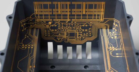
Automotive console prototypes designed and manufactured with IME technology. Source: TactoTek
What’s Driving the Growth of Printed Electronics?
The surge in interest and adoption of printed electronics is driven by several key factors. First, there is an increasing demand for lightweight, flexible, and cost-effective electronic solutions, particularly in consumer electronics, healthcare, and the Internet of Things (IoT). The ability to integrate electronics into everyday objects, such as smart labels or medical patches, has opened up new opportunities for innovation.
Sustainability is another crucial factor fueling this growth. Traditional PCB manufacturing involves complex subtractive etching processes, chemical waste, and expensive materials. In contrast, printed electronics minimize material waste and use energy-efficient additive processes, making them more environmentally friendly. According to IDTechEx, printed and flexible electronics could reduce electronic waste by up to 80% in disposable applications.
Additionally, advances in conductive inks, printable semiconductors, and new substrate materials continue to enhance the capabilities and reliability of printed electronics. Conductive inks based on silver nanowires, for example, have reached conductivity levels of over 10⁶ S/m, making them viable for high-performance circuits even in flexible form factors.
Key Benefits of Printed Electronics
One of the most significant advantages of printed electronics is its cost-effectiveness. Because the circuits are printed rather than etched and assembled, manufacturing costs can be reduced by 30–70% depending on complexity and production volume. The process eliminates the need for expensive substrates like FR4 and minimizes material waste. This makes printed electronics ideal for high-volume, low-cost applications such as RFID tags, flexible sensors, and disposable medical devices.
Flexibility is another major advantage. Traditional PCBs are rigid, which limits their application in wearable and curved-surface designs. Printed electronics, on the other hand, can be integrated into flexible and even stretchable substrates, enabling new form factors for products like smart clothing, foldable displays, and flexible solar panels. Some systems can bend to a radius of less than 5 mm or stretch up to 30% without failure.
Production efficiency also sets printed electronics apart. By using additive manufacturing techniques, multiple electronic layers can be printed in a single process, reducing assembly steps and production time. For example, the complete printing of a simple RFID tag can be accomplished in under 10 seconds, a significant leap compared to traditional etching and assembly.

Printed Electronics Design with Altium Designer. Source: TactoTek
In-Mold Electronics: A Game-Changer for Automotive and Consumer Products
One of the most exciting advancements in printed electronics is in-mold electronics (IME), which combines printed circuitry with injection molding. This technique allows electronic circuits to be directly embedded into three-dimensional plastic components during the molding process. IME technology is revolutionizing industries such as automotive, consumer electronics, and home appliances by enabling sleek, lightweight, and highly integrated designs.
The benefits of in-mold electronics are substantial. Weight savings of up to 60% compared to traditional mechanical assemblies have been reported, which is especially valuable in the automotive industry where reducing every kilogram can increase fuel efficiency by 1–2%. IME also reduces the number of components by up to 70%, significantly cutting down on manufacturing complexity, assembly time, and potential failure points.
In addition, IME supports thinner product designs and improves ergonomics. Capacitive touch buttons, LED lighting, and antennas can all be seamlessly integrated into curved plastic surfaces, enabling intuitive, modern interfaces. Design cycles are also shortened by as much as 25%, thanks to fewer parts and faster tooling iterations.

In-mold electronics packaging. Source: DuPont
Challenges in Printed Electronics Design
Despite its numerous advantages, printed electronics still faces several challenges, particularly in the design and manufacturing process. One major hurdle is the integration of MCAD and ECAD tools. Since printed electronics often require complex three-dimensional designs, traditional electronic CAD (ECAD) tools must work seamlessly with mechanical CAD (MCAD) software to ensure precise alignment and functionality. Misalignments of even 0.1 mm can lead to functional failures in tight, molded assemblies.
Another significant challenge is thermoforming and strain simulation. Many printed electronics applications involve shaping or stretching circuits to fit a specific form factor, such as in-mold electronics or flexible displays. However, conductive traces can crack or lose conductivity when stretched beyond their limits. Accurate simulation tools are needed to predict and mitigate these effects, especially for designs that undergo deformation during or after manufacture. Strain simulations that account for multi-axis deformation are essential for reducing failure rates, which can otherwise reach 15–20% in early design stages.
Material selection also plays a crucial role. Conductive inks, dielectric materials, and flexible substrates must all be carefully chosen based on the application’s mechanical, electrical, and environmental requirements. The lack of standardized material libraries in many ECAD tools adds friction to the development process and increases the risk of design failures, especially in thermally or chemically challenging environments.

Altium Designer Printed Electronics layers isolation support
How Altium Supports Printed Electronics Design
As printed electronics continue to push the boundaries of traditional PCB design, ECAD tools must evolve to meet the unique requirements of this technology. Altium provides a comprehensive set of features tailored for printed electronics, enabling engineers to efficiently design, simulate, and manufacture next-generation electronic products.
One of Altium’s standout capabilities is its integration of design rules specifically optimized for printed electronics. This ensures that conductive traces, crossovers, and layer stacks are compatible with flexible substrates and ink constraints, helping designers avoid costly manufacturing errors.
Altium’s powerful Layer Stack Manager helps manage unconventional stack-ups typical in printed electronics, including multiple printed dielectric and conductive layers. This ensures that designs maintain the necessary mechanical flexibility and thermal characteristics.

Altium Designer Printed Electronics Layer Stack Manager Material Library support
The integrated material library provides various materials for both conductive and non-conductive layers. This simplifies the material selection process and helps ensure design reliability.
Altium Designer's Dielectric Shapes Generator automates the creation of dielectric patterns over crossovers in printed electronics designs. Enabled by the Printed Electronics Crossover Generator extension, it simplifies post-routing tasks and ensures accurate, consistent dielectric shapes.

Altium Designer Dielectric Shape Generator
By providing a unified platform for electrical, mechanical, and material considerations, Altium empowers engineers to move from concept to production more confidently and efficiently—particularly for complex printed and in-mold designs.
The Future of Printed Electronics
Printed electronics is poised to transform multiple industries, from healthcare and automotive to consumer electronics and smart packaging. As the demand for lightweight, flexible, and cost-effective electronic solutions continues to grow, advancements in conductive materials, printing techniques, and ECAD tools will drive further innovation.
With tools like Altium Designer integrating critical design capabilities—such as dielectric shapes generator, layer stack management, and material libraries—engineers can push the boundaries of what’s possible in printed electronics. While challenges like MCAD-ECAD integration and thermoforming simulation remain, ongoing developments in simulation and material science will help overcome these hurdles.
According to market research, the global printed electronics market is expected to reach $43 billion by 2030, growing at a CAGR of over 18%. As more companies adopt printed electronics for their next-generation products, we can expect to see a surge in applications that were previously unattainable with traditional PCB manufacturing. From ultra-lightweight medical sensors to smart surfaces and interactive packaging, the future of electronics is being printed—one layer at a time.
About Author
Related Resources
Table of Contents
- What is Printed Electronics?
- What’s Driving the Growth of Printed Electronics?
- Key Benefits of Printed Electronics
- In-Mold Electronics: A Game-Changer for Automotive and Consumer Products
- Challenges in Printed Electronics Design
- How Altium Supports Printed Electronics Design
- The Future of Printed Electronics
Design to Release, Without the Friction
- Keep reviews tied to the right version
- Reduce handoff confusion and rework
- Spot sourcing and release risk earlier
- Work solo, share when needed
Get Started
Thank you, you are now subscribed to updates.

