Push and Shove Router: How it Works and Why You Need It
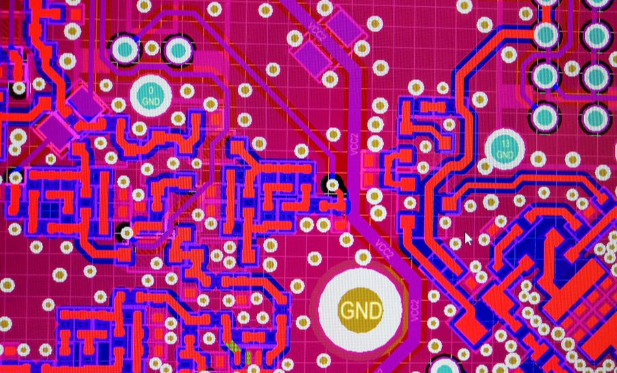
If you have a complex layout like the one shown above, and you need to move traces or vias around the board, what can you do to decrease your routing time? This is where the push and shove router feature in Altium Designer can be a huge help. Using this feature eliminates the need to reroute a large number of unselected traces as you adjust traces and vias in your layout.
So when would you need to use something like this? Doesn’t this interfere with an otherwise pristine layout? As you drag a trace or via, you can easily toggle between different push and shove modes as you move your via or trace around the board. This allows you to accommodate things like additional or replacement components, changes to trace or via sizes, and other layout changes. Toggling between different modes allows you to quickly turn the push and shove features on and off so that you don’t affect any perfect portions of your layout.
Things to Consider When Using a Push and Shove Router with Vias
The push and shove router in Altium Designer is great for quickly moving elements around in a board without manually rerouting surrounding traces. It's a powerful tool that takes advantage of the standard interactive routing features in Altium Designer, but it making the best use of it requires some considerations:
- Multiple layers: Push and shove routing will nudge traces and vias in multiple layers. Therefore, you should use your View Configuration options to make sure you've only turned on the relevant layers.
- Vias: I like this using this feature for when I need to move vias. When dragging vias, the attached traces will follow the via around the board.
- Use early: I think it's best to use this feature early, meaning before you've finalized component placement and any other sensitive traces shouldn't be moved at all. The push and shove router tool lets you focus only on the vias and traces that require movement so that you don't have to do a bunch of manual rerouting.
Let’s look at a couple examples. The image below shows a portion of the example Kame FMU layout in Altium Designer. If you want to access this project, it's available to every Altium Designer user as an example in your Altium 365 Workspace. I've zoomed in on the SPI2_CLK net; this net makes connections on layers 1 and 4, so these are the only layers I've left visible at the moment.

To engage the push and shove router, select the section of the connection you want to move, and then start dragging it. I've selected the via and started moving it towards the right side of the board. As you drag a via or trace around the layout, nearby traces and vias will move out of the way automatically, and the attached traces will drag as well. In this particular example, the two ground vias near the edge and the VCC3 via have moved to make room for the SPI2_CLK via on the outer layer. It may not be obvious, but the internal trace on layer 4 is also moving with the SPI2_CLK via.

As you drag an element around the board, you can hit Shift+R on your keyboard to cycle between the Push Obstacles, HugNPush Obstacles, and Ignore Obstacles modes. This gives you plenty of options for perfecting your resulting routing while gently moving around nearby features in the layout.
If you are not careful, this can leave behind a 90 degree bend or other odd angle; as shown in the image below. In this case, you can drag sections of the traces to clean up the leftover routing, or you can use the gloss tool, and this will leave a nice clean trace leftover. These odd angles will not create signal integrity problems until you start working with extremely high frequencies, but odd angles can act as acid traps if your manufacturer uses a viscous etchant. They also just look messy.

PCB Routing Clearance Rules When Dragging Vias
Another problem which can arise if you are not careful is violation via clearance rules. In fact, because I've left the polygons turned on in the above images, the rule violations will trigger immediately upon placing the via and traces. This is one reason it's best to use this early as you won't have these other features that create clearance violations, so you won't have as much cleanup to do after adjusting your routing. In the example above, you can avoid this simply by shelving your polygons while using the tool and then repouring them later.
In the case of dragging a via that passes through multiple layers, you'll see a rule violation get flagged as the via may touch a net or plane by mistake. The image below shows an example from a different project. I've left the other layers on each side of our desired routing layer turned on so we can see what happens after dragging with the push and shove router. Because we're already in a tight space, a couple things happen:
- There may be leftover holes in upper and lower polygons that need to be filled
- The via might intersect a polygon on a different layer in its new location, creating a clearance violation
- The router will let us drag around the board, but we create some clearance violations when dragging too close to other traces
Thankfully, the automatic DRC tools in Altium Designer will flag clearance violations for you as you drag an element in your layout. This is shown in the image below. There are three violations here: pad-to-trace clearance, trace-to-trace, and pad-to-polygon violations. To quickly reset the polygon fill, use the polygon repour tool, or you can use the T + G + A hotkey in the PCB Editor.
Here, you would also want to drag the SCL via on the same layer, and probably move the SDA via so that you can resolve these clearance violations. Once that's finished, you would need to repour the polygons on the upper and lower layers to fill in the leftover holes and to clear new space for the vias. Because I sometimes have some odd stacked polygons, I don't always use the Repour All Polygons option. Instead I go through and select only the polygons that need to be repoured individually.
Toggling between the different push and shove modes allows you to experiment with different layout configurations as you drag a trace/via. Note that, if you push a trace as you drag, and then switch to Ignore Obstacles mode, the pushed trace will revert to its original location when you started dragging.
Finally, watch out for skew in your nets as you use the push and shove router. If you drag an element around the board and significantly increase the length of a trace, you can induce excess skew in a signal trace. Thankfully, the Matched Length design rule will check for length constraint violations. If a violation does occur, you can use the length tuning features to bring signals back into sync.
Accessing Routing Options in Altium Designer
There are two ways to configure your routing options and tools in Altium Designer:
- In the Preferences dialog
- In the PCB Editor while routing using hotkeys
In order to configure the routing options in Altium Designer, just click on the Preferences option under the Tools menu. Scroll down to the PCB Editor menu in the list on the left-hand side of the dialog. Then click on Interactive Routing. This will bring up a list of options for configuring the routing settings.
In order to configure the modes in the push and shove router, you’ll need to look at the Unselected Via/Track and Selected Via/Track options. This will configure how the dragged element in your layout will interact with nearby tracks or vias. You can toggle between Drag and Move modes in these drop down boxes, which will change how nearby traces are moved around the board as you drag a trace/via in your layout.
You can access other routing options mid-routing by pressing the Tab key on the keyboard. This allows you to change the interactive routing settings while in the middle of a route, including:
- Via pad/hole size mid-route
- Trace width mid-route
- Obstacle avoidance and gloss options mid-route
- Curve or corner settings
- Enable/disable pin swapping
The video below shows how these options can be accessed while using the interactive routing features in the PCB Editor.
More Interactive Routing Tools
The interactive routing tools available in Altium Designer don’t end with the push and shove router. You can easily route multiple signals simultaneously (both single-ended and differential) with Bus Routing, perform pin-swapping with high pin count logic devices, and use a strategic autorouter to cut down on your routing time.
The powerful interactive routing and post-layout analysis tools in Altium Designer® are built on top of a unified rules-driven design engine, allowing you to implement length matching as you use the push and shove router or any of the other layout tools. You’ll also have a complete set of tools for building schematics, managing component information, and preparing deliverables for your manufacturer.
Now you can download a free trial of Altium Designer and learn more about the industry’s best layout, simulation, and production planning tools. Talk to an Altium expert today to learn more.

