Zero-Cross Switching Circuit Designs

A lot of PCB designers work in the DC power domain, and as a result we often talk a lot about DC power monitoring, control, and circuit design. But AC power matters too, and it has its own control techniques that are intended to reduce EMI, provide safety measures for loads and downstream regulators, and modulate power delivery to a load. Zero-cross switching is one such strategy used to help manage EMI and safety in AC power systems
Zero-cross switching manages the timing of power delivery to an AC load in order to reduce electrical noise, prevent inrush current, and ensure safety. It would typically be used with a set of discrete off-the-shelf components, but integrating logic functions into the control strategy would be difficult in many systems without some complex analog circuitry and an ADC.
One strategy that can be used to build more compact zero-crossing detectors is with a programmable mixed-signal device which integrates the required analog and digital logic into a single package. I’ll cover how these designs work in this article.
How Zero-Cross Switching Works
Zero-cross switching is an AC power management technique used for safe and low-EMI switching of AC loads. It is a timing-based AC load control strategy that minimizes electrical stress and interference by switching at an AC signal’s zero-voltage crossing point.
This can be seen by looking at an input AC waveform and the output AC power delivered to a load. Suppose we have perpetually ON input AC power. If we want to deliver AC power to a load, the zero-cross switching circuit can be turned ON at any time, but it will not allow power to flow to a load until the AC input crosses 0V (going low-to-high or high-lto-low). This switching point is shown right at t = 0 in the graph below.
The component being “switched” in this case is most often a triac, relay, or thyristor. The circuit needs to perform the following core functions:
- Detect the state of the AC input
- Switch ON the power delivery path very quickly
- Allow the power delivery path to latch ON
The above graph should clearly illustrate why AC-driven loads may need zero-cross switching: if power delivery to the load was turned ON during any instant where the AC input wave was non-zero, the result would be sudden exposure of the load to high voltage/current. This is what creates the potential for inrush and possible damage to the load circuit or component.
The table below outlines some common uses of zero-cross switching.
| Application | Description |
|---|---|
| Solid-state relays (SSRs) | Many SSRs have built-in zero-cross detectors to switch AC loads only when the voltage crosses zero. This reduces arcing and inrush current. |
| Soft-start in AC motors | For low-power AC motors, zero-cross switching minimizes electrical noise during startup and shutdown. |
| Lighting control (dimmers) | For non-phase-cut dimmers controlling incandescent or resistive loads, zero-cross switching reduces flicker and EMI. |
| Heater control systems | Industrial and residential heater control uses zero-cross switching to avoid voltage spikes when switching resistive loads on/off. |
| Home automation (smart plugs, switches, etc.) | Smart switches that control AC appliances often use zero-cross switching to ensure safe, quiet operation. |
| Triac and thyristor control circuits | Zero-cross triggering of triacs minimizes surge current and EMI bursts, especially when driving inductive loads like transformers. |
| Surge and inrush current limiting | Used in AC power entry circuits (e.g., large SMPS or UPS designs) to engage relays or bypass circuits at the zero-cross moment, which reduces the inrush current. |
Zero-Cross Switching With Discrete Components
There are zero-cross switching circuit topologies that could be built with discrete components. These designs typically require a DC power source and an AC input (possibly rectified), and these designs may involve galvanic isolation.
A very common example is shown in the circuit below:
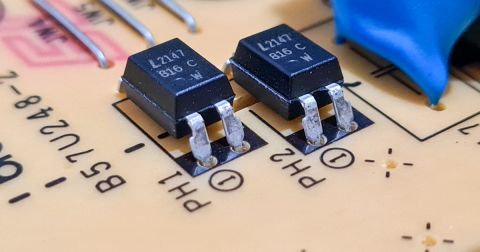
This simple circuit provides galvanic isolation given by the optocoupler’s isolation voltage rating. However, additional components and circuitry are needed to step down the AC voltage to a safe level, before it is brought to the input of the rectifier + optoisolator circuit.
Additional circuit types are available, such as switching a relay, thyristor, or triac with a comparator. Note that FETs are typically not used unless they are push-pull and can be toggled ON simultaneously. A more elaborate example from Texas Instruments for an isolated gate driver circuit is shown below.
Example zero-cross switching detector and logic from the Texas Instruments TIDA-050085 reference design.
Zero-Cross Switching With a Mixed-Signal Processor
Mixed-signal processors are programmable devices (very similar to CPLDs) which consolidate the features and functions in the above examples into a much smaller number of components. Logical processing can be performed on analog signals, which is instrumental in building advanced power management systems that also include zero-cross switching. Because the analog detection and processing can be performed on-chip, it’s possible to implement zero-cross switching with much simpler circuit designs:
- Use the programmable analog comparator to read the AC input
- Use internal LUTs to apply logical conditions for zero-cross switching
- Use a GPIO to toggle power delivery ON
Some additional AC components are typically needed on the interface, particularly in AC power applications (e.g., step-down transformer, low-pass filtering, input impedance buffering). These are quite simple components to implement and still result in a smaller system footprint than the typical case with discrete components.
An example implementation is shown below, where the mixed-signal processor is used with a FET + thyristor to pass an analog signal to a load. The FET + thyristor circuit is very simple and will remain ON as long as the D-latch and LUT logic output a HIGH signal (assuming an n-MOSFET). The programmable VREF signal is then used to set the zero-cross point (i.e., the analog signal’s midpoint voltage).
Once the output GPIO falls LOW (e.g., thanks to the LUT logic), the analog input will drop below the holding current required to keep the thyristor latched ON, and the analog signal will no longer deliver power to the load.
An advantage of a mixed-signal processor is that additional functions like diagnostics and a shutdown sequence can be implemented in the zero-cross switching circuit using the D-latches, GPIOs, and LUTs. If there is some fault in the load or the voltage/current exceeds some safe level, the processor can use its logic output to force OFF the switch and stop power to the load. The additional analog interfaces or GPIOs can also be used to capture data from other sensors or components, which could also be used in logic to determine whether power delivery needs to be halted due to system fault.
This additional level of safety is preferable to the basic approach with discrete components, which requires power cycling the system in the event of a fault. Note that this is also done without a microcontroller; no embedded firmware or memory is needed to implement this mixed-signal processor approach.
PCB Layouts With Zero Cross Switching
PCBs that incorporate zero-cross switching circuits are typically bringing in AC power and must be designed accordingly. These designs might use galvanic isolation with a transformer or isolator in order to step down the AC input to a lower voltage; power is then delivered to the load using zero-cross switching.
- Use best practices for galvanic isolation; separate the primary and secondary sides on each end of an isolating component
- For EMI control, place a Y-type capacitor across the PRI and SEC grounds; this is helpful for experimenting in pre-compliance and can be DNI later
- A digital section may be needed for the system host; separate this part of the system into its own section with dedicated rectification/transformer
- If an earth connection is present, use this with your input EMI filter to handle incoming noise on the power line
- Use large copper rails when high current delivery is required in order to keep conductor temperatures low
The power rail and ground strategies are most important in designs where there is galvanic isolation and a digital section which includes a system host. Even though AC power is being transferred to a load in these designs, the PCB layout will look a lot like an isolated DC/DC converter and similar guidelines will need to be followed.
Note that mixed-signal processors used in these designs will not require a microcontroller or an embedded application; the logic for implementing zero-cross switching can be instantiated the component’s programmable macrocell matrix. This is not the case for other zero-cross switching power management systems, particularly when data must be captured from external sensors (e.g., temperature sensors) over a standard interface like I2C or SPI.
Power electronics relies on safety of components and users, and the Renesas GreenPAK programmable mixed-signal processor product line is instrumental in implementing solutions like zero-cross switching. To learn more, take a look at the GreenPAK components and reference examples.
Whether you need to build reliable power electronics or advanced digital systems, use the complete set of PCB design features and world-class CAD tools offered by Altium to implement your GreenPAK solutions. Altium provides the world’s premier electronic product development platform, complete with the industry’s best PCB design tools and cross-disciplinary collaboration features for advanced design teams. Contact an expert at Altium today!


