Ruminating Rigid-Flex PCB Design

More and more designers are facing the need to reduce size and cost of the products they design, while increasing density and simplifying assembly. Rigid-flex circuits (those which incorporate flexible portions between separate rigid sections) are becoming a more common solution. This blog is the beginning of a short series which discusses the materials, fabrication, and design methods for using rigid-flex technology.
As the title of this blog suggests, I’ve been thinking a lot lately about Rigid-Flex circuit boards. Rigid-Flex can have many benefits, and many designers are at least considering it today who previously did not have to. It seems that more designers are facing higher pressures to build ever more densely populated electronics, and with that also comes pressure to reduce costs and time in manufacturing. Well, this is really nothing new of course. It’s just that the scope of engineers and designers having to respond to these pressures is continuously broadening.
But there are aspects of rigid-flex which could be pot-holes in the road for newcomers to the technology. So it’s wise to first understand how flex circuits and rigid-flex boards are actually made. From there we can look at the design issues and find a clear path forward. For now, let us consider what basic materials go into these boards.
Flex Circuit Materials
Substrate and Coverlay Films
Start by thinking of a normal rigid PCB - the base material is typically fibreglass and epoxy resin. It’s actually a fabric, and although we term these “rigid” if you take a single laminate layer they have a reasonable amount of elasticity. It’s the cured epoxy which makes the board more rigid. This is not flexible enough for many applications though for simple assemblies where there’s not going to be constant movement it is suitable.

For the majority of applications, more flexible plastic than the usual network epoxy resin is needed. The most common choice is polyimide, because its very flexible, very tough (you can’t tear or noticeably stretch it by hand, making it tolerant in product assembly), and also incredibly heat resistant. This makes it highly tolerant of multiple reflow cycles and reasonably stable in expansion and contraction due to temperature fluctuations.
Polyester (PET) is another commonly used flex-circuit material, but it’s not tolerant of high temps and less dimensionally sound that Polyimide (PI) films. I have seen this used in very low cost electronics where the flexible part had printed conductors (where the PET could not handle the heat of lamination), and needless to say nothing was soldered to it - rather, contact was made by crude pressure. I seem to remember that the display in this product (a clock radio) in question never really worked too well due to the low quality of the flex circuit connection. So for rigid-flex we’ll assume we’re sticking to the PI film. (Other materials are available but not often used).
PI and PET films, as well as thin epoxy and glass fibre cores, form common substrates for flex circuits. The circuits must then use additional films (usually PI or PET, sometimes flexible solder mask ink) for coverlay. Coverlay insulates the outer surface conductors and protects from corrosion and damage, in the same way solder mask does on the rigid board. Thicknesses of PI and PET films range from ⅓ mil to 3 mils, with 1 or 2 mils being typical. Glass fibre and epoxy substrates are sensibly thicker, ranging from 2 mils to 4 mils.
Conductors
While the above-mentioned el-cheapo electronics may use printed conductors - usually some kind of carbon film or silver-based ink - copper is the most typical conductor of choice. Depending upon the application different forms of copper need to be considered. If you are simply using the flexible part of the circuit to reduce manufacturing time and costs by removing cabling and connectors, then the usual laminated copper foil (electrodeposited, or ED) for rigid board use is fine. This may also be used where heavier copper weights are desired to keep high-current carrying conductors to the minimum viable width, as in planar inductors.
But copper is also infamous for work-hardening and fatigue. If your final application involves repeated creasing or movement of the flex circuit you need to consider higher-grade rolled annealed (RA) foils. Obviously, the added step of annealing the foil adds to the cost considerably. But the annealed copper is able to stretch more before fatigue cracking occurs, and is springier in the Z deflection direction - exactly what you want for a flex circuit that will be bending or rolling all the time. This is because the rolling annealing process elongates the grain structure in the planar direction.

Figure 2: Exaggerated illustration of the annealing process, obviously not to scale. The copper foil passes between high-pressure rollers which elongate the grain structure in a planar orientation, making the copper much more flexible and springy in the z-deflection.
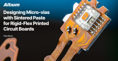
Examples of such an application would be gantry connections to a CNC router head, or laser pickup for a Blu-Ray drive (as shown below).

Figure 3: Flex-circuit used to link the laser pickup to the main board assembly in a Blu-Ray mechanism. Notice that the PCB on the laser head has the flexible portion bent at right angles, and an adhesive bead has been added for strengthening the flex circuit at the join.
Adhesives
Traditionally, adhesives are required for bonding the copper foil to PI (or other) films, because unlike a typical FR-4 rigid board, there’s less “tooth” in the annealed copper, and heat & pressure alone are not enough to form a reliable bond. Manufacturers such as DuPont offer pre-laminated single- and double-sided copper clad films for flexible circuit etching, using acrylic or epoxy based adhesives with typical thicknesses of ½ and 1 mil. The adhesives are specially developed for flexibility.
“Adhesiveless” laminates are becoming more prevalent due to newer processes that involve copper plating or deposition directly onto the PI film. These films are chosen when finer pitches and smaller vias are needed as in HDI circuits.
Silicones, hot-melt glues, and epoxy resins are also used when protective beads are added to the flex-to-rigid joins or interfaces (i.e. where the flexible part of the layer stack leaves the rigid part). These offer mechanical reinforcement to the fulcrum of the flex-to-rigid join which otherwise would rapidly fatigue and crack or tear in repeated use. An example of this is shown in Figure 3 above.

Figure 4: Typical single-layer Flex Circuit stack-up.
It’s important to be aware of the materials used in flexible and rigid-flex circuits. Even though you may generally allow the fabricator freedom to select the materials based on your application, ignorance will not protect you from field-failures of the final product. A really good resource which contains far more detail than my brief introduction here is:
Knowing the material properties will also help in the mechanical design, evaluation and test of your product. If you are working on automotive products for instance; heat, moisture, chemicals, shock & vibe - all need to be modelled with accurate material properties to determine the product’s reliability, and minimum allowed bending radius. The irony is that the driving needs that cause you to choose flexible and rigid-flex are often tied to harsh environments. For example, low-cost consumer personal electronic devices are often subjected to vibrations, dropping, sweat and worse.
Flex & Rigid-Flex Fabrication Processes
At first glance, a typical flex, or rigid-flex board, looks straightforward. However the nature of these requires several additional steps in the build-up process. The beginning of any rigid flex board is always the single or double-sided flex layers. As mentioned last week, the fabricator may begin with pre-laminated flex or may begin with unclad PI film, and then laminate or plate up the copper for the initial cladding. Laminating the film requires a thin layer of adhesive, whereas adhesiveless cladding requires a “seed” layer of copper. This seed layer is initially planted using vapor deposition techniques (i.e. sputtering), and provides the key to which chemically deposited copper is plated upon. This one or two-sided flex circuit is drilled, plated through, and etched in much the same steps as typical 2-sided cores in rigid boards.
The GIF animation below shows the flex circuit board creation steps for a typical double-sided flex circuit.

Figure 5: GIF animation showing flex-circuit build-up process.
1. Adhesive/Seed Coating Applied
Either an epoxy or acrylic adhesive is applied, or sputtering is used to create a thin copper layer for a plating key.
2. Copper Foil Added
Either by RA/ED copper foil lamination to the adhesive (the more mainstream approach) or chemical plating onto the seed layer.
3. Drilling
Holes to vias and pads are most often mechanically drilled. Multiple plated flex substrates can be drilled simultaneously by combining them from multiple reels, drilling between work plates, then rolling out to separate reels on the other side of the drilling machine. Pre-cut flex panels can be combined and drilled between rigid blanks in the same way rigid cores are drilled as well, though it requires more careful registration and the alignment accuracy is reduced. For ultra-small holes, laser drilling is available, though at much added cost because each film has to be drilled separately. This would use Excimer (ultra-violet) or YAG (Infra-Red) lasers for higher accuracy (microvias), CO2 lasers for medium holes (4+ mils). Large holes and cutouts are punched, but this is a separate process step.
4. Through-Hole Plating
Once the holes are made, copper is deposited and chemically plated in the same way as rigid board cores.
5. Etch-Resist Printing
Photosensitive etch resist is coated onto the film surfaces, and the desired mask pattern is used to expose and develop the resist prior to chemical etching of the copper.
6. Etching and Stripping
After exposed copper is etched, the etch resist is chemically stripped from the flex circuit.
7. Coverlay
Top and bottom areas of the flex circuit are protected by coverlay which is cut to shape. There may be components actually mounted on sections of the flexible circuit, in which case the coverlay is also acting as a solder stop mask. The most common coverlay material is additional polyimide film with adhesive, though adhesiveless processes are available. In the adhesiveless process, photoimageable solder mask (the same as used on rigid board sections) is used, essentially printing the coverlay onto the flex circuit. For coarser cheaper designs screen printing is also an option with final curing by UV exposure.

Figure 6: An example of flex-circuit with coverlay - notice that the openings in the coverlay are generally smaller than the component pads.
An important note to make about coverlay is that it is typically only placed on parts of the flex circuit that are ultimately to be exposed. For rigid-flex boards, this means the coverlay is not placed where rigid sections will be, apart from a small overlap - usually about ½ a mm. Coverlay can be included throughout the rigid section, though it adversely affects adhesion and z-axis stability of the rigid board to do so. This kind of selective coverlay is referred to as “bikini coverlay” by the board fabricators that use this process because it just covers the bare essentials. Also, cutouts for component or connection pads in the coverlay leave at least two sides of the pad land to anchor under it. We’ll revisit this in the next blog.
8. Cutting Out the Flex Board
The final step in creating the flex circuit is cutting it out. This is often referred to as “blanking”. The high-volume cost-effective approach to blanking is by using a hydraulic punch and die set, which involves reasonably high tooling costs. However, this method allows punching out of many flex circuits at the same time. For prototype and low-volume runs, a blanking knife is used. The blanking knife is basically a looong razor blade, bent into the shape of the flex circuit outline and affixed into a routed slot in a backing board (MDF, plywood or thick plastic such as teflon). The flex circuits are then pressed into the blanking knife to be cut out. For even smaller prototype runs, X/Y cutters (similar to those used in vinyl sign making) could possibly be used.
Lamination and Routing
If the flex circuit is to form a part of a rigid/flex combined stackup (which is what we are interested in), the process doesn’t stop there. We now have a flex circuit that needs to be laminated in between the rigid sections. This is the same as an individual drilled, plated and etched core layer pair, only much thinner and more flexible due to the lack of glass fibre. As noted previously although, a less flexible layer could be made with PI and glass depending on the target application. Because this is being laminated in with rigid sections, it ultimately has to be framed in a panel that mates with the rigid board panel sections as well.
Laminated Stackups
The flex circuit is laminated into the panel along with the rigid and any other flexible sections, with additional adhesive, heat and pressure. Multiple flex sections are not laminated adjacent to each other. This generally means each flex section has a maximum copper layer count of 2, so that flexibility is maintained. These flex sections are separated by rigid pre-pregs and cores or PI bonding sheets with epoxy or acrylic adhesives.
Essentially, each rigid panel is separately routed out in the areas where the flex is going to be allowed to, well, flex.
Here is an example process of laminating into a rigid-flex board, with two, 2-layer flex circuits embedded between three rigid sections. The layer stack up would look like that shown in figures 3 & 4.

Figure 7: How the Etched, plated, coverlayed and blanked flex panels are combined with the glass-epoxy rigid panels.

Figure 8: Detailed layer stackup showing plated-through holes for each flex section, as well as final through-plated holes in the rigid section.
In the example stack up shown in Figure 8, we have two pre-etched and cut flex circuits, each double sided and plated through. The flex circuit has been blanked into a final assembly panel including boarders for framing - this will keep the flex circuit flat during final assembly after lamination with the rigid panel sections. There are certainly some potential hazards with inadequate support of flex circuit elbows and large open sections during assembly - especially in the heat of a reflow oven. I’ll address some of these issues when looking at the design aspects in my next blog installment.
The coverlay is also applied - like stickers laminated on with adhesive, or by a photo-printing process as mentioned earlier. Once the final flex and rigid panels in this 6-layer stackup are placed together, they are laminated with the outermost (top and bottom) final copper foil layers. Then another drilling for top-to-bottom plated through holes is done. Optionally, laser drilled blind vias (top to first flex, bottom to last flex) could also be made, again adding expense to the design.
The final steps are the printing of the top and bottom solder stop mask, top and bottom silkscreen and preservative plating (such as ENIG) or hot air leveling (HASL).
Multiple Flex Sub-Stacks
While it’s possible to build just about any stackup with rigid and flex sections, it can get ridiculously expensive if you’re not careful to consider the production steps and the material properties involved. One important aspect of flex circuits to remember is the stresses within the materials occurring as the circuit bends. Again, copper is known to be work-hardened and fatigue fractures will occur eventually, with repeated flex cycling and tight radii. One way to mitigate this is to only use single-layer flex circuits, in which case the copper resides at the center of the median bend radius and therefore the film substrate and coverlay are in the greatest compression and tension, as shown in Figure 9.
Because polyImide is very elastic this is not a problem, and will last much longer under repeated movement than multiple copper layers will. Along the same lines, having multiple separate flex circuits is often necessary, but it’s best to avoid having bends at overlapping sections where the length of the flex sections limits the bend radius.

Figure 9: For highly repetitive bending circuits, it’s best to use RA copper in single-layer flex to increase the fatigue life (in cycles before failure) of the copper in the circuit.
Adhesive Beads
As I mentioned last week, there are times when you need to consider using strengtheners where the flex circuit exits the rigid board. Adding a bead of epoxy, acrylic or hot-melt will help improve the longevity of the assembly. But dispensing these liquids and curing them can add laborious steps to the production process.
Automated fluid dispensing can be used, but you need to be really careful to collaborate with the assembly engineers to make sure you don’t end up with globs of glue dripping under the assembly. In some instances the glue must be applied by hand which adds time and cost. Either way, you need to provide clear documentation for the fabrication and assembly folks.
Stiffeners & Terminations
Extreme ends of flex circuits typically terminate to a connector if not to the main rigid board assembly. In these cases, the termination can have a stiffener applied (more thick PolyImide with adhesive) or FR-4. Generally then, it’s convenient to leave the ends of the flex embedded within the rigid-flex sections as well.
The Panel
The rigid flex circuit stays together in it’s panel for the assembly process, so components can be placed and soldered on to the rigid terminations. Some products require components to be mounted also on flex in some areas, in which case the panel has to be put together with additional rigid areas to support the flex during assembly. These areas are not adhered to the flex and are routed out with a controlled-depth router bit (with “mouse-bites”) and finally punched out by hand after assembly.

Figure 10: Final Rigid-Flex panel example. Notice that this one has front and back board edges, and flex circuit, routed out. The rigid sides are V-grooved for snapping off later. This will save time in assembly into the enclosure.
When you're ready to design and build your next rigid-flex circuit board, use the complete set of CAD features Altium Designer®. Once you're ready to release your design data to your manufacturer, you can easily share and collaborate on your designs through the Altium 365™ platform. Everything you need to design and produce advanced electronics can be found in one software package.
We have only scratched the surface of what is possible to do with Altium Designer on Altium 365. Start your free trial of Altium Designer + Altium 365 today.
