Silicon Photonics Integration Challenges in PCB Design
Table of Contents
Silicon photonics will use the same manufacturing processes used in silicon ICs
I was honored to meet Richard Soref at a recent IEEE conference and discuss the current state of electronic-photonic integrated circuits (EPICs). The man is often called “the Father of Silicon Photonics”, and for good reason. If you ask him nicely, he’ll tell you how to build all the fundamental logic gates as photonic circuits directly on silicon.
Now is a landmark time for silicon photonics. Although the technology has been around for decades, it is now on the verge of being heavily commercialized and made available to the masses. There are still some engineering challenges to overcome before silicon photonics can be integrated into systems that run on standard electronic components.
The 100 Gbps+ Challenge in IC and PCB Design
For those who have read this far and are still confused, here is some background: photonic circuits are circuit elements that operate using only light. These circuits are a major topic in the optics and electronics engineering communities. 12 years ago, designers were talking about creating single links that can transfer data at 100 Gbps over copper.
It was found that copper enables data transfer at 100 Gbps over shorter distances, while fiber works best at longer distances. Parallelization can also be used with slower equipment to increase data rates to 100 Gbps and 400 Gbps. The optical equipment required to operate on a 100 Gbps network carries very particular design requirements and is not universally compatible with all electronic components.
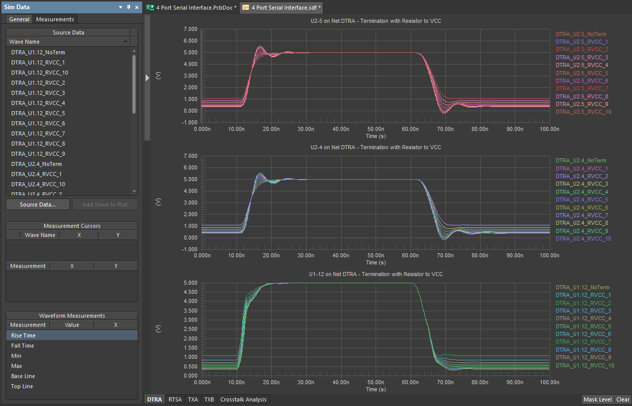
Electrical signal integrity problems in PCBs and ICs become more prominent and noticeable as the data rate increases, and thus the signal rise time decreases. At the IC level, interconnect delay times, propagation delay times, and crosstalk strength all increase as the data rate increases. At the PCB level, crosstalk, radiated and conducted EMI, and thermal management become important high speed design considerations. Optical components offer higher bandwidth solutions that do not suffer from the same signal integrity problems found in electronic components. Greater parallelism in electronic IC design requires higher bandwidth solutions that can be provided by optical components.
Enter photonic integrated circuits (PICs) and electronic-photonic integrated circuits (EPICs). The former type of circuit is designed to operate entirely with light with a large number of photonic elements integrated into a single package. The latter type of circuit is designed to operate using light, but electronic elements may appear in these circuits. Therefore, these circuits can also interface with standard electronic components, depending on the bandwidth of the electronic component.
You might be wondering, why photonics, and why on silicon? The maturity of silicon foundry and chip fabrication capabilities means that these traditional manufacturing processes can be immediately adapted to photonic circuits. If we are going to see PICs or EPICs any time soon, they will most likely be built on silicon photonics technology.
In the future, you’ll likely interface these ICs with PICs and EPICs
Challenges in Silicon Photonics for Use in PCBs
The great thing about silicon is that it is transparent at 1550 nm wavelengths, so it is immediately compatible with optical fiber networking equipment that runs at 1550 nm. This creates another problem in that there are no light sources or detectors in silicon photonics systems made directly from silicon. This is due to the fact that silicon is an indirect bandgap semiconductor.
Integrating a light source and detector directly on a silicon EPIC requires bonding a III-V semiconductor (e.g., InP, InGaAs) or Ge layer directly on silicon. Bonding III-V materials to silicon brings its own technical challenges and remains an active area of research. However, if the operating wavelength is shifted to 2 microns, it becomes possible to build relatively low-loss monolithic silicon EPICs without the use of a III-V material. In either case, this creates two challenges in integrating silicon EPICs onto PCBs to interface with electronic components.
If a III-V material is used as a detector and light source, then interfacing with fiber optic networks requires converting between 2 micron and 1550 nm wavelengths. This will need to be done by placing a standard 1550 nm transceiver somewhere on the board. The bandwidth of the III-V material or the transceiver (whichever is smaller) itself will determine the limiting data rate in this type of system.
If the wavelength in the EPIC is kept at 1550 nm, then this will require placing traditional photodetectors and narrowband infrared LED light sources or laser diodes alongside an EPIC, which presents a challenge in assembly and manufacturing. These components also take up extra board space for each EPIC. It remains to be seen which strategy will be best for integrating EPICs on PCBs. Any light source that is used with silicon EPICs must have fast response time in order to be compatible with the fastest electronics logic families.
The great aspect of silicon EPICs is that switching can be controlled electrically by applying voltage pulses to the chip. This allows external data to be easily input to an EPIC and manipulated within the EPIC. The fact that EPICs do not suffer from the same electrical signal integrity problems as electronics ICs allows an EPIC to be used for faster data processing while still being able to interface with standard electronic ICs. The typical high speed PCB design practices for electronics can still be followed when integrating EPICs on a PCB.
Infrared LEDs
Bringing Silicon Photonics to Life
There are already a number of open source tool sets for designing PICs and EPICs on Si or III-V materials. These component designs can then be sent to an open foundry and manufactured in short runs. Normally, these runs are part of a multi-project wafer (MPW), allowing component designers to manufacture a small number of prototype components while sharing the costs with other designers.
New high power light sources that are integrated into their own PICs (such as multimode lasers), are also a major research topic and are on the verge of early commercialization. Researchers and product developers designing these components can integrate them into a customized evaluation board and examine how they interface with standard electronics ICs. All this will go a long way to advancing adoption and further development of silicon photonics.
The layout and simulation tools in Altium Designer allow you to design PCBs for nearly any application. The component creation tools also allow you to integrate any proprietary or experimental component—including silicon photonics components—into your schematic. You can also include PCB footprints for these components using STEP models designed in mechanical modeling programs.
Contact us or download a free trial if you’re interested in learning more about Altium Designer. You’ll have access to the industry’s best routing, layout, and simulation tools in a single program. Talk to an Altium expert today to learn more.


