Avoid Cross-Board Signal Integrity Issues in High-Performance Multiboard PCB Designs

At a Glance
Avoid cross‑board signal integrity failures in multiboard PCB designs. Learn how connector launches, skew, and boundaries consume margin.


Most signal integrity problems in multi-board systems trace back to boundaries, not to the controlled-impedance runs between them. A connector launch, a cable transition, or a flex-to-rigid junction introduces impedance discontinuities, reference changes, and skew that accumulate across the channel. Engineers who treat each board as an isolated routing problem and defer interconnect decisions to mechanical packaging will find their margin consumed at boundaries they never explicitly designed.
The governing constraint is that every high-speed channel must be budgeted as a complete path from transmitter to receiver, including every transition between boards, connectors, cables, and flex segments. When boundary ownership is ambiguous or undocumented, each board team optimizes locally while no one owns the transitions. The result is a channel that meets no one's impedance or skew budget at the system level.
Signal integrity in multiboard PCB systems must be managed across the entire channel, not just within individual boards. Connector launches, cable assemblies, flex interconnects, and board-to-board transitions introduce impedance discontinuities, skew, and return-path disruptions that consume system margin. Successful multiboard signal integrity design requires end-to-end channel modeling, connector validation, and cross-disciplinary coordination throughout the product lifecycle.
Key Takeaways
- Cross-board signal integrity (SI) failures start at the boundary. Connector launches, reference-path breaks, and interconnect transitions consume link margin each board appears to have, and the assembled channel fails.
- Skew compounds across the system. For parallel interfaces and differential pairs: maintain skew in each board where you have control over routing, before/after connector interfaces, rather than compensating all length/delay mismatches in a single board.
- Understand connector capabilities for high-bandwidth channels. Evaluate connectors based on vendor data and leverage their simulation models to fully evaluate system performance in simulation.
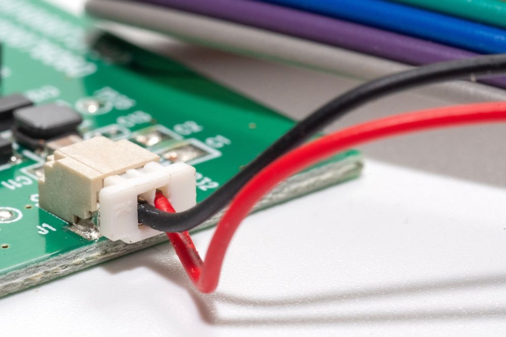
Connector Launch as a Reusable Design Pattern
Most SI escapes happen at transitions, not in the middle of long, well-controlled runs. The connector boundary should be treated as a reusable design pattern, guarded with constraints and review gates so every board team implements the same assumptions. When the launch region is defined by a consistent set of rules rather than left to individual judgment, the same performance carries across designs.
In high-speed PCB design, connector launches often represent the largest impedance discontinuities in the signal path and should be treated as critical signal integrity structures rather than simple mechanical interfaces.
At minimum, the design pattern should enforce:
- Interface definition: standard, target data rate, topology map covering boards, connectors, cable or flex segments, and reference changes.
- Skew budgets: intra-pair and lane-to-lane, allocated per segment.
- Connector rules: pin-map constraints, ground pin interleaving, breakout routing, and via usage.
- Change triggers that require a boundary re-check: connector swap, stackup change, cable length change, board relocation, or enclosure changes near the interconnect.
With these elements locked down, the launch region becomes a constrained design block rather than an ad-hoc routing exercise. If a differential pair changes layers at the launch, keep the transition symmetric: same via structure, same fan-in/fan-out, same layer usage on both legs.
Mechanical Constraints That Affect Channel Performance
Stack height, alignment tolerance, bend constraints, and service routing are channel constraints, not purely mechanical concerns. Mechanical decisions directly affect signal integrity performance in multiboard systems because they alter channel length, impedance behavior, and timing relationships between interconnected boards.
A cable reroute that adds 50 mm of length or changes a bend radius modifies delay and potentially coupling. A board relocation that shifts connector mating height can change via stub length or require a different stackup transition.
Capture these relationships in the ICD so that a mechanical change automatically triggers a boundary re-check. Without this linkage, mechanical teams make changes that look benign from a packaging standpoint but silently erode SI margin.
| Change Category | Example | Channel Impact | Required Action |
| Connector/launch | Family swap, pin-map revision, mating height change | Impedance discontinuity, stub length, breakout geometry | Re-simulate launch, update ICD, re-check skew budget |
| Stackup/structure | Material change, via structure revision, backdrill decision | Impedance shift, reference transition behavior | Re-run impedance and TDR models, verify launch symmetry |
| Mechanical/routing | Cable length change, bend radius, board relocation | Delay shift, coupling change, mating geometry | Re-validate skew budget, confirm connector alignment |
| Retimer/redriver placement | Channel segmentation change | New compliance point, altered loss budget | Re-partition channel, update ICD segment definitions |
Signal Integrity Channel Modeling
To build a comprehensive channel model, cascade S-parameter blocks from the transmitter to the receiver. Each segment of the channel, including the package, board routing, via launches, connectors, and cables, requires a specific model type.
- Use transmission-line models for uniform traces
- Apply S-parameter blocks for discontinuities and connectors
- Convert individual S-parameters to T-matrices and multiply them in sequence
- Run compliance simulations (insertion loss, return loss, eye diagram, COM) to identify dominant segments affecting the loss or reflection budget
- Correlate with TDR and VNA measurements once hardware is available
- Document all model assumptions (Touchstone files, pin maps, stackup, launch geometry) in the interconnect control document
- Regenerate affected models and rerun simulations when boundary conditions change
Discrepancies between simulation and measurement usually trace back to launch geometry differences, connector variability, or dielectric properties deviating from datasheet values. Change one variable at a time when iterating. Treating connector boundaries as fixed abstractions across board revisions is a reliable way to erode SI margin without realizing it until prototype measurements reveal the problem.
System-Level SI Gates for Multiboard Designs Checklist
Before Layout
- Build interconnect models for the
- Lock in connector orientation and mating assumptions for the first layout pass.
- Assign an owner for the end-to-end link.
During Layout
- Standardize connector launch geometry: padstacks, antipads, stitching, and reference continuity.
- Control via stubs in connector fields.
- Track skew against the system budget and keep tuning away from launches unless explicitly allowed.
Before Prototype Release
- Run a boundary-first review: mapping, launch, return-path continuity, skew allocation, and mechanical constraints.
- Confirm the assembled channel matches the assumed topology: board locations, stack height, cable or flex length, and bend constraints.
- Define bring-up validation conditions: cable sets, fixtures, and assembly variables.
After Bring-Up
- If the link fails, audit boundaries first: pin map and orientation, launch geometry, reference continuity, and segment skew.
- Log every change that touches the interconnect path and re-run the boundary review when a trigger fires.
Keeping Multiboard Context Visible with Altium Agile Teams
System-level SI spans electrical, mechanical, and sourcing realities. Altium Agile Teams keeps that multiboard context visible as the system evolves, so teams can catch boundary changes before layout and packaging decisions lock.
Design reviews happen in the design context. If a mechanical change shifts a connector and breaks a channel assumption, the electrical team sees it early. Connector and cable decisions can be made alongside live availability and risk data from Octopart, supporting earlier lock decisions on boundary-defining parts. Change tracking stays tied to the design state, so connector swaps and stackup revisions stay visible to the right stakeholders.
For more details, see Altium’s documentation on synchronizing a multiboard assembly. It’s a useful next step for formalizing how multiboard relationships should be captured and kept up to date. Learn more about Altium Agile Teams →

About Author
Related Resources


Related Technical Documentation

Table of Contents
Speed at Scale. Structured Repeatability. Secure Flexibility.
- Start up fast with out‑of‑the‑box workflows
- Collaborate using ECAD‑MCAD codesign tools
- Manage BOMs with live supply chain part data
- Manage access and security as teams scale
Contact Us
Thank you, you are now subscribed to updates.