


Most Common Causes of PCB Assembly Rework and Scrap

At a Glance
Learn about the most common causes of PCB assembly rework and why bare PCBs get scrapped.


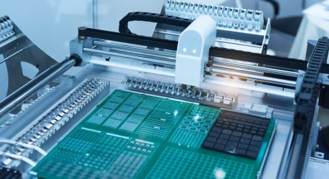
There is a lot that can go wrong during PCB assembly. When procuring printed circuit boards and PCB assemblies, simple things like incorrect BOM line items and footprint mismatches can force an assembly to be delayed, reworked, or scrapped. Some of the features in a PCB layout can also increase the chances of defects which will require a fabricated PCB to be scrapped. PCB fabricators will put a design through a DFM review, but a DFM review is not a guarantee of high yield.
In my experience, I have found some common factors that lead to scrapping PCBs or reworking PCB assemblies. I'll outline these common factors in this article.
PCB Scrap
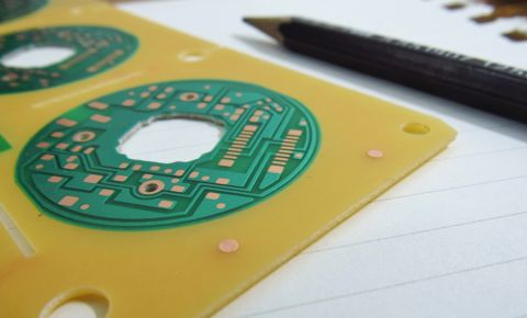
When a PCB has defects during fabrication, it will need to be scrapped. There really is no way to rework a bare PCB that has fabrication defects. PCB fabrication defects generally produce open circuits or short circuits where you did not expect them, and there will be very little chance that the PCB assembly will work as designed.
The table below outlines some causes of PCB scrap and some solutions for preventing scrap.
| Defect | Cause | Prevention/Solution |
|---|---|---|
| Open circuit between trace and via | Insufficient annular ring | Increase the via pad size |
| Short circuit between trace and plane | Insufficient anti-pad | Increase hole wall or pad edge to plane clearance |
| Shorts across different net pads during assembly | No solder mask dam | Increase pad-to-pad clearance or reduce mask expansion |
| Exposed copper at board edges | Insufficient board edge clearance | Increase board edge clearance |
| Intermittent open circuit at vias | Fractured via plating | Reevaluate process or allow for thicker plating |
| Blind via annular ring breakout in heavy copper | Excessive wander during drilling | Increase via pad size or use wrap-over plating on sub-laminations |
| Garbled designators or labels in silkscreen | Silkscreen font is too small | Increase silkscreen size |
Incorrect pad arrangement which does not match any component footprint, wrong footprint in the PCB library, review and change the footprint as required
Of course, this is not a complete list of fabrication defects, but I have seen all of them at some point. Manufacturers should perform a comprehensive DFM review in order to identify the risks I outlined in the table above. However, some manufacturers will not perform a comprehensive review of the design unless you specifically request it. CBA buyers should be aware of what they are getting when they order manufacturing and assembly services.
If a board is destined to be scrapped, then the best time to scrap the board is before it ever goes into assembly. In addition to a DFM review before PCB fabrication, their PCBs should go through some electrical testing. The fastest and simplest electrical test is continuity testing, which measures the presence of opens and shorts. This is then compared with your netlist export from your PCB design software. Buyers who are creating orders with a PCB fabrication house should also request this service as the charge required to set up such automated tests is very inexpensive.

PCB Assembly Rework
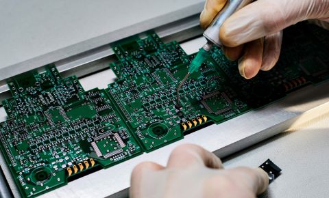
In contrast with fabricated bare printed circuit boards, PCB assemblies can be reworked and modified to some extent. PCB assembly rework can be as simple as touching up or cleaning solder joints on accessible pads, or as complex as completely desoldering and replacing selected components. More advanced rework involves detaching and cleaning BGA or LGA contacts, as well as reballing BGAs for another round of assembly.
There are many common causes of assembly defects which can be addressed with rework, and not all of those issues are the fault of the designer. Some of the common causes are:
- Solder bridging across components due to low clearances
- Uneven reflow profile, leading to tombstoning
- Skewed components due to excessive paste or slow cool down of solder
- Solder flow through unfilled holes and vias, such as thermal bias
- Solder voiding on large die-attached pads
- Insufficient deposition, particularly on small SMD package leads
- Warpage defects on leadless packages, such as head-in-pillow in BGA packages
- Excessive solder flux residue, including from no-clean flux, which requires further cleaning
This also is not an exhaustive list of potential PCB assembly defects, but they happen to be common reasons that boards may be sent back to an assembler for rework. PCB assemblers should perform certain inspections to identify assemblies which will require rework, typically consisting of visual inspection with AOI, X-ray inspection of leadless components, and a final cleaning step.

What Can PCB Buyers Do?
PCB buyers have a responsibility to understand the capabilities of their suppliers and audit their suppliers for quality. At low volume or in prototyping runs, this is less important, but it becomes more important as production runs scale in size. Every scrapped board and rework step equates to lower yield on the factory floor, and increases the chances that a less reliable assembly ends up deployed in the field.
Different companies perform different audit levels and have different reliability requirements which might exceed some of the common industry quality standards, such as ISO 9001 and AS9100. Aside from auditing the processes and procedures on the factory floor, buyers should also be aware of the inspections and quality expectations required from engineers. These should be communicated to PCB suppliers; when these requirements can't be met, it's time to consider using a different supplier.
Whether you need to build reliable power electronics or advanced digital systems, use Altium’s complete set of PCB design features and world-class CAD tools. Altium Develop provides the world’s premier electronic product development platform, complete with the industry’s best PCB design tools and cross-disciplinary collaboration features for advanced design teams. Experience Altium Develop today!
About Author
Related Resources
Related Technical Documentation
Table of Contents
Design to Release, Without the Friction
- Keep reviews tied to the right version
- Reduce handoff confusion and rework
- Spot sourcing and release risk earlier
- Work solo, share when needed
Get Started
Thank you, you are now subscribed to updates.

