


Export Native Designs With a PCB-to-Gerber Converter

At a Glance
Whether you’re starting from scratch or modifying a previous design, Altium Designer’s PCB-to-Gerber converter gives you the greatest PCB file format flexibility.


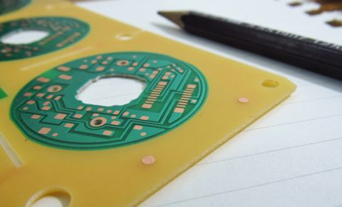
Gerber files serve as the fundamental bridge between PCB design and manufacturing, encoding circuit board layouts into a format that fabrication equipment can interpret and execute. Named after the Gerber Scientific photoplotter company that pioneered the technology in the 1960s, these files have evolved significantly over the decades to meet the increasingly complex demands of modern electronics manufacturing.
While traditional Gerber formats remain widely used, most commonly the RS-274X format, newer intelligent formats promise to eliminate many of the communication gaps, manual processes, and potential errors that plague conventional workflows. Understanding the capabilities and limitations of each format is crucial for making informed decisions about design handoff strategies that can significantly impact manufacturing efficiency, quality, and time-to-market.
Alternatives to Gerber RS-274X
There are four primary Gerber file formats in use today, though one is obsolete. The evolution includes the obsolete RS-274-D format, the popular Gerber RS-274X format, the improved Gerber X2 format, and the newest Gerber X3 format released in 2020. The Gerber X2 and X3 formats contain layer stack-up information, which was not contained in previous Gerber file format versions. Each successive format has addressed limitations in its predecessors while maintaining backward compatibility.
Gerber RS-274X remains the de facto standard format for printed circuit board design software, utilized for fabricating about 90% of all PCBs designed today worldwide. Yet despite its popularity, Gerber comes with a number of practical limitations, which can lead to a variety of problems throughout the fabrication process. The open standards Gerber X2, Gerber X3, IPC-2581, and ODB++ were developed to address the problems inherent in RS-274X. What can these newer formats do that RS-274X can't? Let's take a closer look at these formats to understand the advantages they provide over the industry standard.
Gerber X2
The Gerber X2 comes from an expanded version of the GerberX format, which now includes design data, in addition to layout image data. Whereas previously, board layer order and stack-up information had to be manually interpreted and verified, now this data is included within the X2 fabrication files. Also included within the X2 fabrication files is a set of drill files detailing the drill size, location, plated/non-plated, and layer span. Note that a specific viewer (CAM tool) is required to read all of the additional information in Gerber X2 files.

Gerber X2 output for a multilayer PCB. Note the embedded mechanical drawing information into hte output files.
Gerber X3
Released in 2020 by Ucamco, the Gerber X3 format represents a significant leap forward for the Gerber family. While maintaining the familiar multi-file export structure (one per layer), X3 uniquely integrates component and assembly data directly into Gerber exports, traditionally requiring separate design output files. This integration supports bill of materials data, pick and place information with reference designators and part numbers, and assembly attributes. This advancement helps prevent common issues like footprint mismatches between fabrication and BOM data, streamlining the handoff to assembly.
However, Gerber X3 still lacks advanced features found in competing formats, such as complete layer stack-up definitions, impedance control requirements, or embedded design rules. Consequently, CAM-based analysis still necessitates manual definition and arrangement of the layer stack during process planning and DFM review.
ODB++
ODB++ is an intelligent data format that consolidates all fabrication and assembly data into a single compressed archive. Unlike Gerber formats, which use multiple individual files, ODB++ streamlines data management and transfer by packaging manufacturing, assembly, and design data into one comprehensive archive. This approach clarifies manufacturing intent by explicitly defining pads, nets, and components; this is one reason it is my favorite format for creating simulations (e.g., in Simbeor) and performing PCB manufacturing reviews.

ODB++ archive review in CAMtastic!
One major advantage of ODB++ is the inclusion of additional information, such as:
- Complete layer stack-up information
- Impedance control requirements
- Embedded design rules
- Bill of materials
Just as is the case with the newer Gerber formats, the PCB viewer software needs to have the relevant feature included and the ODB++ export must include the information listed above in order to be useful in a CAM tool.
Despite these technical benefits, ODB++ has seen limited adoption in the industry, possibly due to concerns about format ownership or the need for specialized software, even with ongoing efforts to maintain its openness.
IPC-2581
The IPC-2581 standard was initiated, developed, and driven by contributors from a wide range of PCB industry segments, such as OEMs, PCB Fabricators, and Contract Manufacturers, as well as MES, PLM, and CAD/CAM vendors. In addition to graphical image data, IPC-2581 goes above and beyond to consolidate all aspects of a design, from layer stack-up and materials to assembly and test details, into a single data format, contained in a single file.
In addition to generating a complete set of fabrication data, IPC-2581 also generates assembly data. The Pick & Place information can specify a location in X/Y and Z locations, as well as component polarity and rotation. This enables support not only for embedded components but for stacked components as well. In addition, IPC-2581 supports netlist and test point data generation, to facilitate in-circuit, functional, or JTAG testing.
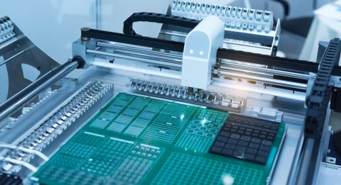
Generating Gerber Files and Alternatives
Gerber files or alternatives to Gerber RS-274X are generated using the PCB-to-Gerber converter feature in your PCB design software. All design software has this feature with support for the RS-274X format, but only some platforms support the newer formats and alternatives. There are alos Gerber-to-GCode converter tools and open-source tools like Gerbv. Altium's PCB design solutions provide an integrated generator and viewer for Gerber and ODB++ files directly from the PCB layout. You can also generate other standard deliverables in a variety of file formats for your manufacturer.
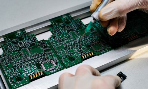
Once you’ve finished your circuit board layout, your manufacturer will review your manufacturing outputs to ensure conformance to their manufacturing process and capabilities before production. Altium will take your PCB layout and instantly export manufacturing files in standard formats, including the other important deliverables for production and assembly (BOM, pick & place, drill files, and drawings). See a step-by-step tutorial of the process for generating Gerber files in Altium Designer.

Generating fabrication outputs in Altium's PCB design environment.
Whether you want to use the standard Gerber format or alternatives to RS-274X, you can customize the PCB-to-Gerber file converter feature in Altium to define non-functional pad removal and decimal precision. Whether you need to build reliable power electronics or advanced digital systems, use Altium’s complete set of PCB design features and world-class CAD tools. Altium provides the world’s premier electronic product development platform, complete with the industry’s best PCB design tools and cross-disciplinary collaboration features for advanced design teams. Contact an expert at Altium today!

About Author
Related Resources
Related Technical Documentation
Table of Contents
Design to Release, Without the Friction
- Keep reviews tied to the right version
- Reduce handoff confusion and rework
- Spot sourcing and release risk earlier
- Work solo, share when needed
Get Started
Thank you, you are now subscribed to updates.