


Best Software For PCB Design For Manufacturing (DFM)

At a Glance
The best software for PCB design for manufacturing is often not a separate application. In many cases, it is the rule engine already built into your PCB layout tool.


Experienced PCB designers understand that DFM is not a final review step performed before release. It is a design methodology that shapes decisions from stackup definition through final routing. When fabrication and assembly constraints are embedded directly into the layout environment, many common defects are prevented before manufacturing data is ever generated.
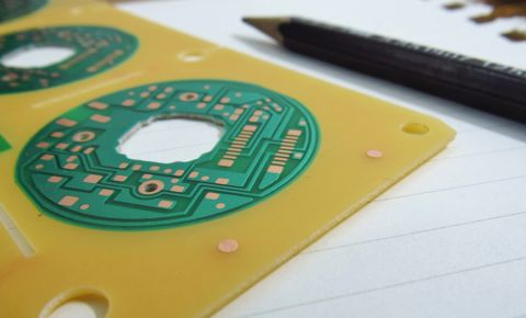
Modern PCB layouts are often too complex to rely on manual review in order to catch all DFM violations. Manufacturability constraints originate from fabrication tolerances, drill limitations, solder mask registration accuracy, copper balance requirements, assembly clearances, and package-specific geometry. The best software for PCB design for manufacturing must allow these constraints to be defined numerically and enforced consistently throughout the layout process.
Start With the DRC Engine in Your ECAD Tool
The most effective software for PCB design for manufacturing is the design rule checking system built into your PCB layout environment. When configured properly, the DRC engine becomes the primary enforcement mechanism for fabrication and assembly limits.
Design rules are commonly thought of as electrical constraints, such as impedance control or differential pair spacing. However, the same rule system also enforces manufacturability requirements. Minimum trace width, copper clearance, annular ring size, drill diameter, solder mask expansion, and component spacing are all numerical limits that reflect a PCB fabricator’s published process capabilities. When these values are defined at the beginning of a project, the layout tool continuously evaluates geometry during placement and routing.
Most modern PCB design tools allow manufacturability rules to be defined in two primary ways: broad category-based rules and object-to-object constraint rules. Both approaches embed fabrication limits directly into the design database rather than leaving them to be discovered after layout.
Category-Based DFM Rules
Category-based rules apply manufacturability limits to defined groups of objects. A minimum trace width or copper clearance value is entered once and then applied to a scoped set of layers, nets, or component classes. As routing progresses, every segment is evaluated automatically against those limits.
This method is efficient because it mirrors how fabrication capabilities are typically published. A manufacturer will specify minimum trace width, minimum copper-to-copper clearance, minimum finished hole diameter, and minimum solder mask sliver. These parameters can be translated directly into rule definitions that govern all objects in the layout.

Because rules can be scoped by layer, net class, via type, or component grouping, designers can apply different manufacturability limits within different regions of the board. For example, fine-pitch BGA fanout regions may require different via geometries than mechanically drilled through-holes in low-density areas. Category-based rules provide structure without requiring each object to be individually configured.
Constraint-Based (Matrix) DFM Rules
Constraint-matrix systems allow manufacturability limits to be defined between specific object pairs rather than across broad categories. Instead of one global clearance rule, spacing can be defined between selected net classes, layer pairs, or object types. This approach provides additional granularity when fabrication requirements vary within the same design.
For example, high-voltage nets may require larger spacing than low-voltage logic signals. Blind vias spanning certain layer pairs may require different aspect ratio limits than mechanically drilled vias. By defining these relationships numerically in a structured table, the layout tool evaluates each interaction according to its specific pairing.

This method becomes especially useful in high-density or mixed-technology designs where standard global rules are insufficient. Constraint tables centralize all electrical and physical limits, allowing designers to audit manufacturability parameters directly against fabrication documentation. Instead of relying on memory or informal guidelines, the design database becomes the authoritative record of manufacturing intent.
|
Feature |
Category-Based Rules |
Constraint-Based (Matrix) Rules |
|
Primary Scope Method |
Applied to object groups (layers, nets, classes) |
Applied between specific object pairs |
|
Typical Use Case |
Global fabrication limits (minimum trace width, global clearance, hole size) |
Specialized constraints between selected nets or regions |
|
Granularity |
Broad and efficient |
Highly granular and specific |
|
Ease of Setup |
Faster to configure for standard designs |
Requires more detailed configuration |
|
Best For |
Standard multilayer PCBs with consistent fabrication limits |
Mixed-technology boards, high-voltage regions, HDI sections |
|
Manufacturing Alignment |
Mirrors typical fabrication capability tables |
Mirrors engineering-level constraint documentation |
|
Maintenance Complexity |
Easier to audit at a high level |
Easier to control nuanced interactions |
In practice, many designs use both systems simultaneously. Category-based rules establish baseline fabrication limits, while constraint-based rules refine specific interactions where standard global values are insufficient. Together, they form the foundation of effective PCB design for manufacturing software inside the layout environment.
Post-Layout Software for PCB Design For Manufacturing
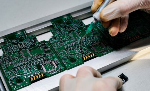
After layout is complete, the design is exported into manufacturing formats. At this stage, the PCB manufacturer does not examine the native ECAD database. Instead, they import fabrication data into CAM software to perform their own DFM analysis.
The minimum data set typically includes:
- Gerber files for copper and mask layers
- NC drill files for each layer span
- IPC-D-356 netlist
These files allow automated measurement of copper features, drill hits, mask openings, and connectivity. CAM software verifies that the generated outputs reflect fabrication tolerances and that no geometry falls below minimum capability limits.
This stage does not replace internal rule enforcement. Instead, it validates that exported manufacturing data accurately reflects the intended design.
Gerber, ODB++, and IPC-2581 Viewers
Advanced CAM platforms used by PCB fabrication companies provide deeper rule-based inspection of manufacturing outputs. These tools allow custom rule sets to be defined according to the manufacturer’s process limits. Automated error reports highlight violations in copper geometry, drill spans, mask registration, and net connectivity. These systems represent the same type of analysis that fabricators perform before approving a job for production.
In addition to full CAM platforms, standalone viewers are available for examining manufacturing data before release to fabrication. These tools allow designers to open Gerber, ODB++, or IPC-2581 files independently of the native ECAD database, providing a neutral inspection of the exact data that will be delivered to the manufacturer.
Gerber viewers graphically inspect copper, solder mask, silkscreen, and drill layers, verifying polarity, feature spacing, and alignment. ODB++ viewers add structured manufacturing data, including drills, net connectivity, and stackup, in a directory format. IPC-2581 viewers offer similar functionality via a single structured archive encompassing fabrication, assembly, stackup, and component metadata.

By reviewing Gerber, ODB++, or IPC-2581 outputs in a standalone viewer, designers validate the integrity of exported manufacturing files independent of the layout tool. This extra verification step helps ensure that the fabrication data accurately reflects design intent before submission for production.
DFM Begins in Your PCB Layout Software
No standalone CAM application can replace properly configured design rules. The most effective software for PCB design for manufacturing remains the rule engine embedded in the layout environment. Post-layout tools are valuable for validation, but prevention occurs inside the PCB layout software itself.
When manufacturability constraints are defined at project startup and enforced throughout placement and routing, fewer violations reach fabrication. Late-stage modifications decrease, fabrication delays are minimized, and engineering time is preserved.
Whether you need to build reliable power electronics or advanced digital systems, use Altium’s complete set of PCB design features and world-class CAD tools. Altium provides the world’s premier electronic product development platform, complete with the industry’s best PCB design tools and cross-disciplinary collaboration features for advanced design teams. Contact an expert at Altium today!

About Author
Related Resources
Related Technical Documentation
Table of Contents
Design to Release, Without the Friction
- Keep reviews tied to the right version
- Reduce handoff confusion and rework
- Spot sourcing and release risk earlier
- Work solo, share when needed
Get Started
Thank you, you are now subscribed to updates.


