


You Don't Always Need Pull-up Resistors on SPI Lines

At a Glance
Pull-up resistors are not required on SPI lines. There are certain instances where they can be used without affecting the functionality of the push-pull buffer.


There is a popular misconception that pull-up resistors are always required or necessary on the lines in a SPI bus. I am here to tell you unequivocally that pull-up resistors are not always required on an SPI bus in order for it to perform its basic function of sending and receiving digital data.
The buffer in an SPI interface has a push-pull topology which (at a high-level) involves high-side and low-side switching MOSFETs, essentially forming a CMOS inverter. As we will see in this article, the presence of pull-up resistors has no impact on the basic switching functionality of a push-pull bus.
That being said, there are instances where it makes sense to place a pull-up resistor on a push-pull bus, and in some datasheets a component manufacturer will recommend it or require it. We’ll look at these situations and how it affects your system behavior. While there can be more elaborate solutions that eliminate the need for pull-up resistors in these situations, placement of a pull-up resistor can be a solution that keeps your design simple and provides insurance that the interface will work correctly.
How an SPI Bus Works With Pull-Up Resistors
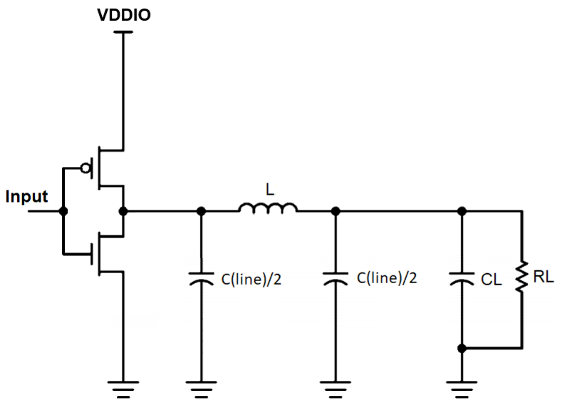
Let’s take a look at the typical model of a buffer in an SPI interface. All SPI buffers have a push-pull topology that consists of high-side and low-side switching which drives a signal onto the bus, and each signal in the SPI bus (CS, MOSI, MISO, and SCLK) will have this topology. An example of this circuit is shown below. Note that a real SPI buffer is not as simple as two MOSFETs, but the same idea applies in general.
CMOS inverter as an SPI driver. The output connects to a trace (represented as lumped elements) and a load circuit (RC equivalent model).
The entire reason for using this topology is for the discharging capacitances in the buffer circuit to provide reasonably fast edge rates on the output, which will be much shorter than the clock period on the bus. This is what allows for faster data rates than an open-drain protocol (e.g., I2C).
An SPI bus that includes pull-up resistors is essentially a CMOS inverter driver with a resistor in parallel with the high-side FET in the output buffer. Now let’s see what happens during each switching state in the driver and we can see what happens on the bus.
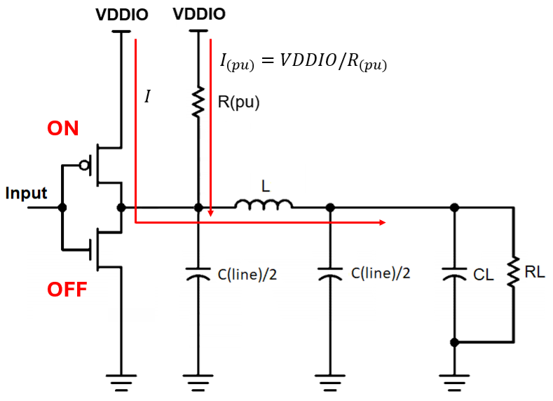
Logic HIGH Output
During the logic HIGH output state, the NMOS is OFF and the PMOS is ON. VDDIO is now sourcing current into the connected trace and load. The capacitance in the trace and the load then begin charging up until the voltage seen at the load matches VDDIO. Here, the ON-resistance of the PMOS is on the order of mOhm, while the pull-up resistor is on the order of 1 to 10 kOhms. Obviously, the pull-up resistor is so large that it is essentially being short circuited by the PMOS in the HIGH logic output state.
Because all the current flows through the PMOS in the HIGH logic state regardless of the presence of the pull-up resistor, the switching characteristics will be unaffected.
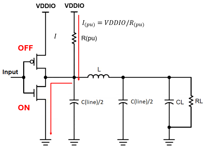
Logic LOW Output
Now let’s consider that the circuit has switched to the logic LOW output state. In this state, the NMOS is ON and the PMOS is OFF, so the trace and load capacitance are discharging through the NMOS into the GND net. Because the PMOS is off, it appears as a very high resistance (order of MOhms) that is much larger than the value of the pull-up resistor (1 to 10 kOhms).
Because the pull-up is the smaller resistor in this case, it will permit a current value of VDDIO/R(pu) to flow to the NMOS. For a 1 to 10 kOhm pull-up resistor and VDDIO = 3.3 V, the leakage current into the NMOS would be 0.33 to 3.3 mA. This is much smaller than the typical SPI current of ~50 mA, so again we will not notice any effects on switching characteristics. The fall time on the bus will be limited by the load and trace capacitances, the output resistive impedance of the buffer circuit, and the ON-state resistance of the NMOS.
If Switching is Unaffected, Why Use a Pull-Up?
Clearly, the placement of a pull-up resistor on an SPI line does not affect its ability to drive a signal onto the bus. Therefore, the pull-up should be performing some other function that is not related to data transmission, otherwise the resistor would not be used.
The reasons for using a pull-up resistor on one or more lines in an SPI interface vary depending on the proposed situation. Some situations where pull-up resistors are used include:
- Placement on the CS line for a peripheral device
- Placement on the MISO line for a host device
- Placement on the MOSI line for a peripheral device
- Placement on all bus lines near the output pins
The stated reasoning for placement in any of these situations is to set the logic state on one of the peripheral components in the bus. The most common recommendation is to place a pull-up resistor on the CS pin of a peripheral in order to pull it high. If the peripheral has an active low enable pin, then this will always pull the pin high unless the driver side of the pull sets the pin low.
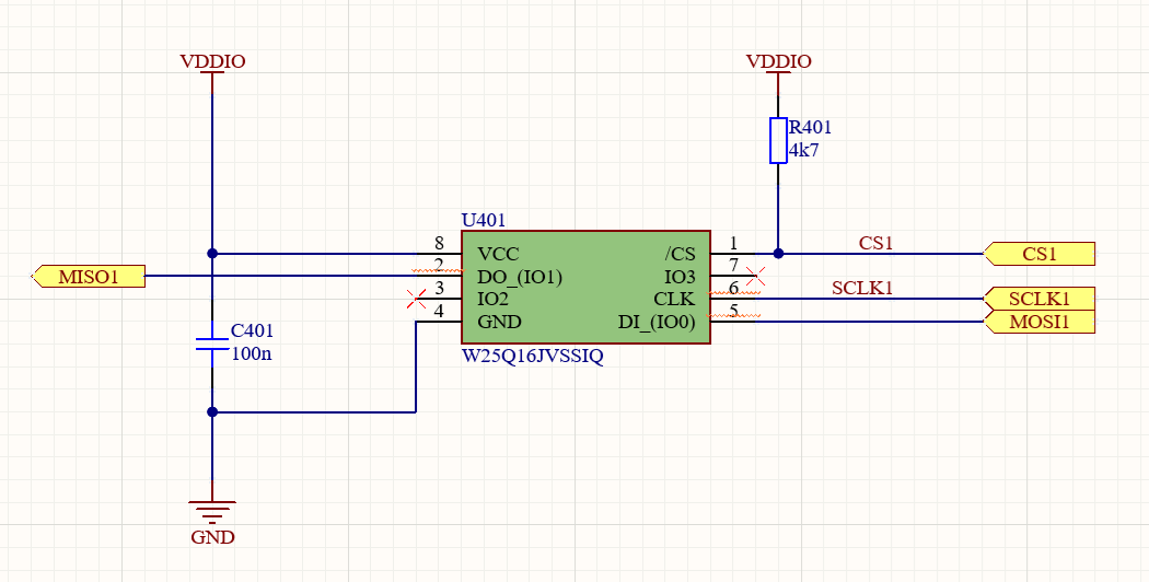
An example of such usage is shown below. In the PCB layout, the pull-up resistor would be placed close to the CS pin of this peripheral.
Typical placement of a pull-up resistor on the CS pin of a SPI bus.
Why would this be used? The stated reason is that during system startup, the CS pin could be floating in any state and this would create a risk that noise can corrupt data on the bus. Furthermore, if the host device starts up before the peripheral and the CS pin becomes enabled unintentionally, the host could start manipulating data in the peripheral. This is sometimes cited as a reason to place a pull-up on memory peripherals.
To date, I cannot find a compelling reason to place a pull-up resistor on the SCLK (clock) line (unless it is stated to do so in a datasheet). The reason is that the receiving logic circuit will not toggle if other conditions (specifically CS line state) are not met regardless of the presence of a clock signal. Some app notes and datasheets recommend the MISO or MOSI pull-up resistors for various reasons, but testing whether this works is simple and the resistor can always be de-soldered when working your prototype.
Follow the Datasheet
If the datasheet for your component explicitly states to include a pull-up resistor on a particular SPI pin, then you should follow this advice. This is based on the intent of the chip design engineer, often for the case of multifunctional pins and/or to set the pin state in the case of a disconnected pin. This is not a PCB layout guideline, it's a simple circuit functionality guideline: if the datasheet says to place the pull-up resistor then you should place it.
The reverse is not true: you are not required to place a pull-up resistor on an SPI line in order for it to function. If the datasheet does not explicitly mention placing a pull-up resistor on one of the SPI pins, then it is not strictly required for the pins/interface to function. In this case, consider the cases discussed above and whether they will apply to your particular system.
Power Sequencing Is a More Elaborate Solution
Because this is most often cited as a problem with the CS pin state during system startup, I think power sequencing between peripherals and the system host would be the best approach to prevent this problem during startup. In smaller systems, there may not be space in the device available for multiple regulators or for a power sequencer that can pass through the required power. It’s a simpler solution to place a pull-up resistor, but understand that these pull-up resistors are not required for the interface to function correctly.
Whether you need to build reliable power electronics or advanced digital systems, use the complete set of PCB design features and world-class CAD tools in Altium. To implement collaboration in today’s cross-disciplinary environment, innovative companies are using Altium to easily share design data and put projects into manufacturing.

About Author
Related Resources
Related Technical Documentation
Table of Contents
Design to Release, Without the Friction
- Keep reviews tied to the right version
- Reduce handoff confusion and rework
- Spot sourcing and release risk earlier
- Work solo, share when needed
Get Started
Thank you, you are now subscribed to updates.

