

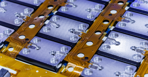



Flex Circuit Termination: What Happens at the Edge Matters More Than You Think

At a Glance
Learn about flexible circuit terminations in fully flexible PCBs and rigid-flex designs. The termination style you use will impact reliability.


Ask most designers where flex circuits fail and they'll tell you the bend zone. Honestly, that's a fair answer. Bend radius, copper geometry, and dynamic versus static flexing are key concerns and get a lot of attention.
But termination failures? Those come back more than people expect and require more precision than it might appear. Common issues that point to termination issues include ZIF tails that won't insert consistently, solder joints that crack after a few months in the field, or contact resistance creeping up with no obvious cause.
It makes sense. The termination zone is where a compliant, flexible material meets something rigid and unforgiving: a connector housing, a solder joint, a bonded substrate. That transition doesn't naturally cooperate with flex circuit mechanics, and if the design doesn't account for it, something in the assembly will inevitably show you.
Key Takeaways
- Flex circuit terminations need focused review because many reliability issues begin at the connector or soldered edge.
- ZIF tails require controlled finished thickness, coverlay placement, surface finish, and stiffener details.
- Direct solder connections need strain relief so motion is carried by mechanical support instead of solder joints.
- Fabrication drawings should define dimensional limits, material requirements, and inspection criteria.
- First-article checks should verify the termination area before the design moves into production.
ZIF Connector Tails: Tight Tolerances with Big Consequences
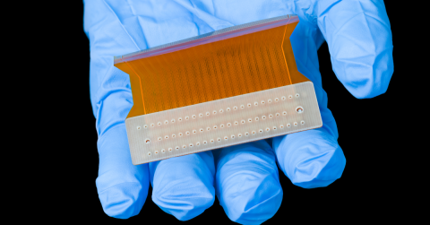
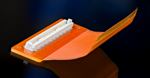
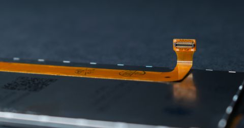
Zero insertion force (ZIF) connectors show up everywhere: consumer electronics, medical devices, automotive, industrial controls to name just a few. The termination design looks simple enough: a row of pads, a defined thickness, a coverlay edge that stops at the right place. In practice, every one of those elements has less margin than one would think.
Thickness is the one that seems to surprise people most, and I can see why. It doesn't feel like it should be complicated. ZIF connectors accept a flex tail within a specific thickness window, usually 0.2mm or 0.3mm total, and the tolerances don't leave much room. Polyimide, adhesive, copper, coverlay film, and stiffener all stack up to that final number. Calculate it, confirm it against the connector spec, and get it worked out with your fabricator before the stack-up is finalized. It is all too common to inadvertently not include the adhesive thickness for coverlay and the polyimide stiffener in the equation.
Changing it afterward is painful. I've seen it require a full redesign of the stiffener stack when caught too late, and depending on material availability, it can hit lead time too. That’s not a fun conversation to have with a customer.
Coverlay edge placement is equally unforgiving. If the edge lands too close to the pads, adhesive creep during lamination bleeds onto the pad surface, and you get inconsistent contact resistance. If it is too far back, the copper at the transition zone is unprotected. Talk to your fabricator about their actual registration capability and design your tolerance budget around what they can reliably hold.
Surface finish needs to be specified explicitly. Don't leave it as a fabricator judgment call. ZIF contacts rely on metal-to-metal contact, so ENIG works well in most applications. If you're anticipating thousands of insertion cycles though, that's a conversation worth having with your supplier before you default to it. Hard gold over nickel may be the better call.
The stiffener needs to be fully defined on the drawing too: material, thickness, size, and bonded area. An undersized stiffener lets the tail buckle on insertion. Wrong adhesive or incorrect positioning and the tail thickness varies across the width, which makes connectors behave in unpredictable ways that are hard to analyze after the fact.
Direct Solder Termination and Strain Relief
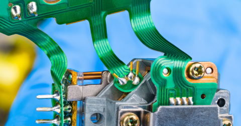
Some flex circuits get soldered directly to a rigid PCB, and it's a legitimate approach when it's designed for it properly. The issue is that solder is rigid and flex is not. Every time the assembly moves during handling, installation, or normal service life, the solder joints at that termination edge absorb a bending moment. Do that enough times and the joint fatigues.
Strain relief geometry needs to be in the design from the start. Copper traces approaching the termination pads should transition gradually and smoothly with no sharp bends or right-angle turns close to the solder joint. The flex circuit should be mechanically constrained near the termination through a stiffener, an enclosure feature, or a dedicated hold-down. Bending stress needs somewhere to go. Make sure it's the constraint absorbing it, not the solder joint.
Mechanical anchor pads are worth adding in any application that sees real handling stress or vibration. They're copper pads soldered purely for mechanical adhesion, and they take the peel forces that would otherwise attack the signal pads. That is most often a worthwhile trade.
The Fabrication Drawing Is Key
Communication through the fabrication drawing is very critical and requires extra attention. The design intent is there, but if the fabrication drawing doesn’t fully capture it, assumptions, including incorrect assumptions, can easily be made.
As an example, a fab drawing that shows pad geometry and coverlay outlines but doesn’t specify thickness tolerances, surface finish, stiffener bondline location, or coverlay edge registration tolerance leaves those decisions to the fabricator. Fabricators are experienced and will make reasonable calls, but they don't always have the full picture of how the design will be used or what the connector vendor actually requires.
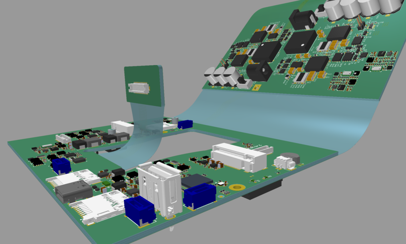
The documentation needs to define at minimum: final flex tail thickness and tolerance accounting for every layer in the stack-up, coverlay edge location, and the allowable positional tolerance relative to the contact pads, surface finish type and plating thickness, and stiffener material, size, and bonded area. If your current drawing template doesn't have fields for these items, that's something worth fixing before the next flex project goes out the door.
First Article Checks Worth Making
When the first articles come back, slow down on the termination zone. Measure the flex tail thickness at several points across the insertion zone, not just one location. Variation across the width can cause as many problems as being out of spec overall. If you have a connector on hand, do a test insertion before anything goes to assembly.
Look at the coverlay edge under magnification. Is the adhesive boundary clean and consistent across the full width? Is there any sign of plating at the contact area? This may not be obvious at normal inspection distances, but could have an impact on reliability and performance.
Before You Release the Design
A few things worth confirming before this goes to fabrication.
- Have you calculated the full flex tail thickness and checked it against your connector spec?
- Is the coverlay edge location and tolerance explicitly called out on the fabrication drawing, not just visible in the CAD file?
- Is the surface finish specified by name in the fab notes?
- Is the stiffener fully defined including material, thickness, size, and bonded area?
- And if you're going to direct solder, is anything actually constraining the flex near that termination, or are the solder joints doing all the work?
A quick review before releasing the design can have a big impact.
When those questions are answered and the design is ready to go, the next place things break down is usually the handoff itself: a reviewer looking at an older version, fab notes updated in one place but not reflected elsewhere, feedback arriving in an email thread nobody can find later. Altium Develop keeps the design, review comments, and release outputs in one place so that when you're ready to release, you're not spending time reconciling versions or chasing down approvals.
Get started with Altium Develop →
Frequently Asked Questions
What Is the Most Common Flex Circuit Termination Risk?
The largest risk is an uncontrolled transition from compliant flex material into a rigid connector, board, or soldered interface. Finished thickness, support, and registration errors can all create intermittent contact or early mechanical fatigue.
How Should a ZIF Tail Thickness Be Specified?
Specify the final measured thickness and tolerance on the fabrication drawing, including copper, dielectric, adhesive, coverlay, and any stiffener. The connector datasheet should be the controlling reference for the allowable range.
Why Does Coverlay Placement Matter Near Contacts?
Coverlay location controls where insulation and adhesive stop relative to exposed pads. If it is too close, adhesive can reach the contact area; if it is too far away, copper near the transition can lose protection.
When Should a Stiffener Be Used?
Use a stiffener when the flex tail must stay flat during insertion, clamping, or handling. It is especially important for ZIF connectors and for soldered terminations that need load sharing near a rigid interface.

About Author
Related Resources
Related Technical Documentation
Table of Contents
Solutions for Every Role and Team
- Discover and evaluate design options earlier
- Develop in one shared workspace
- Scale with control and compliance
- Connect every stage of hardware development
Learn More
Thank you, you are now subscribed to updates.