




Comparing Flex and Rigid-Flex PCBs: When to Use What?

At a Glance
Compare flex and rigid-flex PCBs across cost, bend radius, and impedance. Choose the right construction before layout locks in your constraints.


Flexible and rigid-flex PCBs have become essential components in modern electronic design, offering unique advantages for applications requiring space-saving, durability, and dynamic capabilities. Yet, for PCB designers new to these technologies, choosing between flex, rigid-flex, and traditional rigid PCBs can be daunting. This blog provides information to help understand the key differences, advantages, and ideal use cases for these types of PCBs, helping you make informed decisions for your next project.
Flex and rigid-flex constructions get specified for the wrong reasons more often than most teams admit. The decision tends to start from a mechanical wish, a thin wearable, a folding hinge, a tight enclosure, and the electrical and manufacturing consequences get worked out afterward. That sequence is backwards. The construction you choose sets your bend radius limits, your layer transition behavior, your controlled impedance options, and your fabrication yield long before you place a single component.
Key Takeaways
- Choose the construction type before layout begins. Flex and rigid-flex get specified for the wrong reasons. The construction you choose sets bend radius limits, layer transition behavior, controlled impedance options, and fabrication yield before a single component is placed.
- Flex and rigid-flex solve different problems. Flex suits lightweight, dynamic, or conforming geometry applications where repeated motion is a requirement. Rigid-flex suits compact multi-region assemblies where eliminating board-to-board connectors justifies engineering the rigid-to-flex transition carefully.
- The rigid-to-flex transition is the highest-risk region in a rigid-flex design. Layer transitions, copper anchoring at the boundary, and stress concentration at the rigid edge are where these designs fail in the field, not in the rigid or flex zones themselves.
- Engage your fabricator before routing. Flex fabrication differs fundamentally from rigid fabrication. Bend radius limits, stiffener placement, impedance feasibility across the transition, and Class 2 versus Class 3 acceptance criteria must be resolved with the fabricator before layout, not discovered during first article inspection.
Flex and Rigid-Flex Construction
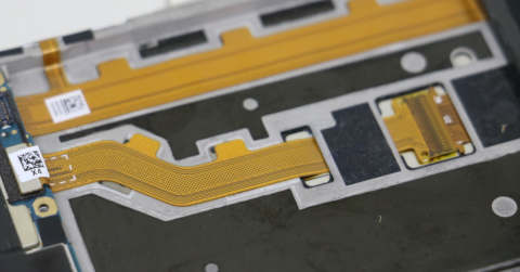
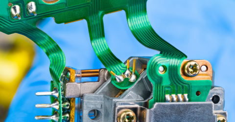
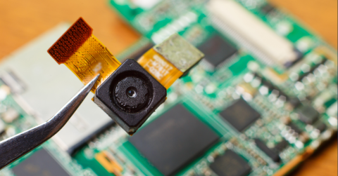
Flexible PCBs, often referred to as flex circuits, are thin, lightweight circuit boards designed to bend and twist into non-traditional shapes. A flex circuit is a thin conductor stack on a polyimide base, with copper laminated and protected by coverlay rather than soldermask over a rigid core. Flex PCBs lack the rigid substrates found in traditional boards, allowing them to fit into designs with irregular geometries. The absence of a rigid substrate is what lets it conform to a curved surface or survive repeated motion.
Main Features of Flex PCBs
- High flexibility and lightweight structure
- Can bend, fold, or twist without breaking
- Excellent for dynamic applications that involve movement or vibration
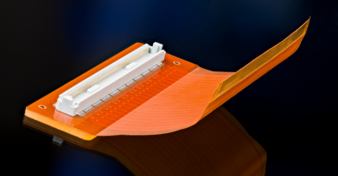
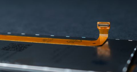
Flex designs can conform to curved shapes while still connecting to other devices through standard connectors.
Rigid-flex combines rigid sections built on conventional laminate with flexible sections that carry signals between them. Rigid-flex PCBs combine rigid and flexible layers into a single board, providing the structural integrity of rigid PCBs with the adaptability of flex circuits. The integration eliminates board-to-board connectors and the cables that go with them, which removes a known population of failure points. In exchange, you inherit the rigid-to-flex transition as the highest-risk region of the board. Layer transitions, copper anchoring at the boundary, and stress concentration at the rigid edge are where these designs fail in the field.
Main Features of Rigid-Flex PCBs
- A hybrid design integrating rigid sections for stability and flexible zones for adaptability
- Enhanced durability, especially in harsh environments
- Space-efficient and reliable, reducing potential failure points caused by interconnects
Flex vs. Rigid-Flex vs. Rigid PCBs: Construction Trade-Offs at a Glance
Flex | Rigid-Flex | Rigid | |
Bare-board cost | Moderate | High | Low |
System assembly cost | Moderate | Low in multi-interconnect designs | High with multiple boards plus connectors |
Dynamic bend capability | High with RA copper, single-layer bend | Limited to flex regions | None |
Controlled impedance | Constrained by thin polyimide stackup | Manageable in rigid regions, harder across transition | Well controlled |
Dominant design risk | Strain relief and handling | Rigid-to-flex transition | Connector and interconnect reliability |
Best fit | Lightweight, dynamic, conforming geometry | Compact multi-region assemblies, harsh environments | Static, cost-sensitive designs |
Factors to Consider When Choosing Between Flex and Rigid-Flex PCBs
To decide which technology to use, consider the following:
- Mechanical Requirements
- Do you need flexibility, bending, or movement? Opt for flex PCBs.
- Do you require flexibility and stability in specific zones? Choose rigid-flex.
- Space Constraints
- Flex PCBs are ideal for highly compact spaces.
- Rigid-flex designs work well for compact yet complex assemblies.
- Cost Considerations
- Flex PCBs are more cost-effective for simpler applications.
- Rigid-flex PCBs, while expensive, reduce assembly costs in multi-layer designs.
- Environmental Conditions
- Flex PCBs can handle vibration but are less durable under extreme conditions.
- Rigid-flex PCBs offer superior performance in harsh environments.
- Assembly Complexity
- Rigid-flex PCBs simplify assembly and reduce interconnects.
- Flex PCBs may require additional connectors for integration.
By weighing factors such as mechanical demands, cost, and environmental conditions, PCB designers can select the ideal solution for their specific needs. As technology continues to advance, the applications for flex and rigid-flex PCBs will only grow, making them indispensable tools for modern electronics.
Compliance, Documentation, and Fabricator Engagement
Flex and rigid-flex carry documentation and compliance obligations that rigid boards do not. These constructions are governed by IPC-6013 for performance and qualification, with IPC-6011 establishing the general reliability framework, and Class 2 versus Class 3 selection drives acceptance criteria, coupon requirements, and inspection.
Regulated work adds requirements such as AS9100D for aerospace quality systems. Inspecting and testing a three-dimensional rigid-flex assembly is harder than testing a flat rigid board, and the test and inspection method has to be planned during design rather than discovered in first article inspection.
The single most effective step is engaging the fabricator before layout. Flex fabrication is a fundamentally different process from rigid fabrication, and shops differ in their methods, material sets, and achievable geometries. A pre-layout conversation should resolve the items that constrain the design before any routing happens.
- Bend radius limits tied to your copper weight and layer count
- Stiffener placement, surface finish, and aspect ratio limits
- Controlled impedance feasibility across the rigid-to-flex transition
- Minimum line and space, via sizes, and clearances in the flex region
- Class 2 versus Class 3 acceptance criteria and the resulting coupon and inspection plan
Selecting between flex and rigid-flex comes down to matching construction to the governing constraint rather than to the application label. Specify flex when the design needs genuine flexibility, dynamic motion, or weight reduction in a conforming envelope, and accept that strain relief and handling become your primary concerns. Specify rigid-flex when a compact multi-region assembly justifies removing connectors, and you are prepared to engineer the transition region carefully. Resolve bend radius, stackup, impedance, material CTE, and class requirements with your fabricator before layout, and the construction will hold up in manufacturing and in the field.
From Construction Decision to Release Confidence
Choosing between flex and rigid-flex before layout begins is one of the highest-leverage decisions in hardware development. Get it right and your fabrication constraints are locked in before a single trace is routed. Get it wrong and the rework compounds.
That rework loop is exactly the kind of friction Altium Develop is built to reduce. When your construction choice is made early and documented clearly, the rest of the design process moves with less ambiguity.
Altium Develop gives hardware designers and small teams a clearer path from design to review to release. The rigid-flex and flex design capabilities are built into the same Altium Designer environment engineers already trust so the workflow supports the work instead of surrounding it. If you're specifying flex or rigid-flex on your next project, use Altium Develop to keep the design, the review, and the release outputs connected from the start.
Frequently Asked Questions About Flex and Rigid-Flex PCBs
What is the minimum bend radius for a flex PCB?
The minimum bend radius depends on layer count, copper weight, and whether the board bends dynamically or is folded once during installation. For dynamic bend designs, where the board flexes repeatedly in service, use a bend radius of at least 100 times the material thickness and no more than two layers. For one- to two-layer designs, a bend radius of at least 6x the flex thickness is the baseline; designs with three or more layers require at least 12x. Always confirm these limits with your fabricator before layout, since material sets vary by shop and affect what's achievable.
Where do rigid-flex PCBs fail in the field?
The rigid-to-flex transition zone is the most common failure point due to stress concentration at the boundary. Copper anchoring at the rigid edge, layer transitions, and via placement near the flex interface are where fatigue and delamination originate, not in the rigid or flex zones themselves. Vias create particular challenges because the plated barrel that creates electrical connectivity also creates a rigid structure; stress concentrates at the via edges until the barrel cracks, which is why vias should never be placed in areas that will bend.
Is rigid-flex more expensive than using separate rigid boards with connectors?
The bare-board cost of rigid-flex is higher than a standard rigid PCB, but total system cost tells a different story. Rigid-flex eliminates connectors and assembly steps, so upfront fabrication cost is higher while total system cost may be lower. The savings compound in high-reliability applications where connector failures drive field returns, warranty costs, and rework cycles. The business case for rigid-flex strengthens as the number of board-to-board interconnects in the design increases.
Can rigid-flex PCBs support controlled impedance?
Yes, but the approach differs across regions of the board. Rigid-flex can support high-speed and high-reliability applications when the stackup, materials, and routing are engineered to preserve controlled impedance, continuous return paths, and stable dielectric behavior through both rigid and flex regions. Impedance is well-controlled in the rigid sections and manageable in static flex areas; the rigid-to-flex transition is where it becomes harder to maintain because the dielectric thickness and material properties change. Resolve impedance targets with your fabricator before routing, not during design review.

About Author
Related Resources
Related Technical Documentation
Table of Contents
Solutions for Every Role and Team
- Discover and evaluate design options earlier
- Develop in one shared workspace
- Scale with control and compliance
- Connect every stage of hardware development
Learn More
Thank you, you are now subscribed to updates.



