Getting Started with PCB Design

NOTE: This Guide was written for Altium Designer 18. For the latest Altium Designer has to offer, please visit https://my.altium.com/altium-designer/getting-started.
This tutorial will start with a sketch of a circuit and will take you through the process of representing the circuit as a schematic, implementing the circuit as a printed circuit board, and generating the outputs required for board fabrication.
This tutorial is based on an astable multivibrator design. New users of Altium software may find value in reading the article Exploring Altium Designer for an explanation of the interface, information on how to use panels, and guidelines for managing design documents.
GETTING STARTED WITH PCB DESIGN
The design that will be captured and implemented as a printed circuit board (PCB) is a simple astable multivibrator. The circuitis shown below; it uses two 2N3904 transistors configured as a self running astable multivibrator.

Astable Multivibrator Circuit Sketch
Capturing (drawing) the schematic is the first step of the tutorial, but first a project must be created.
CREATING THE PCB PROJECT
The PCB project is the set of design documents (files) required to specify and manufacture a custom PCB circuit board. More information about managing and creating Altium projects can be found here.
1) Create a New PCB Project. File » New » Project » PCB Project.
2) Use File » Save Project As… to save the new project. Choose or create the project directory and save the project withthe name Multivibrator.

Create a New PCB Project
3) The project name will appear in the Projects panel.

Projects Panel
ADDING A SCHEMATIC TO THE CIRCUIT BOARD PROJECT
1) Right-Click on Multivibrator.PrjPcb and select Add New to Project » Schematic.
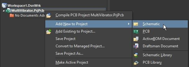
Create a New Schematic Sheet for the Circuit

Schematic Sheet in Projects Panel
2) To save the new schematic sheet, select File » Save As or select Save . Type the name Multivibrator in the File Namefield and click Save. (The file extension *.SchDoc is automatically added).
When the blank schematic sheet opens, the main menu bar and related buttons change in context for schematic entry displaying the Active Bar in the workspace. The Active Bar is displayed in all document editors in Altium Designer and provides placement controls for PCB, schematic, Draftsman, and library objects at your fingertips. Also, you can customize many aspects of the workspace including repositioning and customization of panels and toolbars.

Schematic Document Active Bar
Active Bar icons which have a triangle in the lower right allow you to right-click on them to select different objects for placement:

Bus Entry on Schematic Document Active Bar
SETTING SCHEMATIC SYMBOL PREFERENCES
Before composing the circuit, set up the appropriate document options by completing the following steps:
1) Set the sheet size to Letter as shown in the following guide:

Setting Page Size in the Preferences Panel
To make the document fill the viewing area, select View » Fit Document (shortcut: V, D). Save the schematic by clicking Save or selecting File » Save (shortcut: F, S).
PLACING THE COMPONENTS ON THE SCHEMATIC DIAGRAM


Setting Page Size in the Preferences Panel
Refer to the rough schematic sketch above for the general layout of the circuit, and place 2N3904 transistors Q1 and Q2.
1) Display the Libraries panel by clicking the Panels button at the bottom right of the software, and select Libraries.

Opening the Libraries Panels
2) Find the 2N3904 transistor in the panel by either scrolling through the component list or by using the search button.
3) Click on the 2N3904 entry, then click the Place button. The cursor will change to a cross hair and you will have an outlined
version of the transistor floating on your cursor. Do not place the transistor yet!
4) Before placing the part on the schematic, press the Tab key to open the properties panel and pause placement. In the Properties section of the dialog, type Q1 into the Designator field.
5) Continue placement by clicking on the pause button that is displayed in the center of the schematic. Once the transistor is in the desired position, left mouse click or press Enter on the keyboard to place the transistor onto the schematic.
6) The system remains in component placement mode with the part outline floating on the cursor. Place the second transistor. Because it is the same as the previous one, the software will automatically increment a component’s designator.
7) Referring to the rough schematic diagram shown before, notice that Q2 is drawn as a mirror of Q1. To flip the orientation of the transistor that is floating on the cursor, press the X key on the keyboard. This flips the component horizontally (along the X-axis).

Properties Panel During Part Placement
8) Move the cursor to position the part to the right of Q1. To position the component more accurately, press the PageUp keytwice to zoom in two steps. You should now be able to see the grid lines.
9) Once positioned, left mouse click or press Enter to place Q2. Once again, a copy of the transistor attached to the cursorwill be placed on the schematic, and the next transistor will be floating on the cursor ready to be set.
10) Exit part placement by clicking the Right Mouse Button or pressing the ESC key. The cursor will revert to a standard arrow.

Mirrored Transistors Placed On Schematic Sheet
Placing the Resistors
Place the four resistors into the schematic.
1) The Properties panel will be used frequently for the remainder of this tutorial. Dock the Properties panel to the left sideof the workspace.
For additional information on panels see: Working with Panels in Altium Designer
2) In the Libraries panel, make sure the Miscellaneous Devices.IntLib library is active.
3) Set the filter by typing res in the filter field below the library name.
4) Click on Res1 in the components list to select it, then click the Place button. The resistor symbol is floating on the cursor.
5) Without changing any additional properties, place the four resistors as shown below.

Resistors Placed on Schematic Sheet
6) Using the rough design below as a reference, select each resistor in the schematic and change the Designator and Valueproperties of each resistor by clicking on the resistor and updating the fields in the Properties panel.

Astable Multivibrator Circuit Sketch
7) The Value property updated in the above step is used for circuit simulation. The Name property is typically used to identify the component on the schematic and in downstream reports such as a Bill of Materials. By entering =Value in the Name property, the resistance set in the Value property is echoed to the Name property. Select all four resistors by clicking with the Shift key down.
8) The Properties panel now reflects the parameters that are all common across the four resistors. Change the Name property to =Value and the Name property will reflect the resistance set in Value across all selected resistors as shown below.

Name Set to Value Parameter of Resistors in Properties Panel
9) Finally, with all four resistors remaining selected, scroll down to the Value property and click on to turn visibility off. The four resistors will reflect the change.

Resistor Value Parameter Visibility Turned Off
Placing the Capacitors
Place the two capacitors.
1) The capacitor part is also in the Miscellaneous Devices. IntLib library, which should already be selected in the Libraries panel.
2) Type cap in the component’s filter field (located below the
selected library) in the Libraries panel.
3) Click on Cap in the components list to select it, then click thePlace button. The capacitor symbol is floating on the cursor.
4) Press the Tab key to edit the capacitor’s attributes. In the Component Properties dialog set the Designator to C1, the Name to = Value, set the Value property to 20nF, and disable the visibility of the Value parameter.

Capacitors Placed on Schematic Sheet
5) Using the image below as a guide, position and place the two capacitors in the same way that you placed the previous parts. Right-click or press ESC to exit placement mode.
Placing the Connector
Place the two capacitors.
1) Select Miscellaneous Connectors.IntLib in the Libraries panel. The required connector is a two-pin socket; type *2into the Libraries panel filter field.

2-Pin Header in Libraries Panel
2) Select Header 2 from the parts list and click the Place button. Press Tab to edit the properties and set Designator to Y1.
3) Before placing the connector, press X to flip it horizontally so that it is in the correct orientation. Click to place the connectoron the schematic, as shown in the image below.
4) Right-click or press ESC to exit part placement mode.
5) Save your schematic by selecting File » Save from the menus (shortcut: F, S) or clicking save .

2-Pin Header in Libraries Panel
MAKING CIRCUIT CONNECTIONS
Referring to the sketch of the circuit below, use the place wire command to create connectivity between circuit elements.

Astable Multivibrator Circuit Sketch
1) To provide a good view of the schematic sheet, press the PageUp key to zoom in or PageDown to zoom out. Alternatively, hold down the Ctrl key and roll the mouse wheel to zoom in/out, or hold the Ctrl + Right Mouse button down and drag the mouse up/down to zoom in/out.
2) Choose the place wire command from the Active Bar (highlighted below) and wire the lower pin of resistor R1 to the base of transistor Q1 in the following manner by positioning the cursor over the bottom end of R1. A red connection marker (large cross) will appear at the cursor location indicating that the cursor is over a valid electrical connection point on the component.

Place Wire Command from the Active Bar
3) Click the Left Mouse Button or press Enter to anchor the first wire point. Move the cursor and a wire will extend from the cursor position back to the anchor point. The default corner mode is a right angle, the tip box below explains how to change the corner mode. Right angle is the best choice for this circuit.
4) Position the cursor over the base of Q1 until you see the cursor change to a red connection marker. Click or press Enterto connect the wire to the base of Q1. The cursor will release from that wire.
Note: The cursor remains a cross hair, indicating that the system is ready to place another wire. To exit placement mode completely and go back to the arrow cursor, Right-Click or press ESC again. Do not exit at this time.
5) Add connections for the remaining elements of the circuit, as shown in the figure below. When finished placing all connections, right-click or press ESC to exit placement mode. The cursor will revert to an arrow.

Complete Schematic Sheet Wiring
NETS AND NET LABELS
Complete the following steps to place net labels on the two power nets.
1) Select Place Net Label from the Active Bar (highlighted below). A net label will appear floating on the cursor.

Place Net Label from Active Bar
2) To edit the net label before it is placed, press the Tab key to pause label placement and go to the Properties panel and enter 12V in the Net Name property and continue placement of the label.
3) Place the net label so that the bottom left corner of the net label touches the uppermost wire on the schematic, as shown in the image below. The cursor will change to a red cross when the net label is correctly positioned to connect to the wire. If the cross is light grey, it means there will not be a valid connection made. See the net label in free space (left image) and positioned over a wire (right image) below.

Incorrect Vs. Correct Placement of Net Labels
4) After placing the first net label, net label placement mode will remain active. Press the Tab key again to edit the second netlabel before placing it. Type GND in the Net Name property.
Place the net label so that the bottom left of the net label touches the lower most wire on the schematic (as shown in the image below). Right-click or press ESC to exit net label placement mode.
5) Select File » Save (shortcut: F, S) to save your circuit. Save the project as well.

Saved Completed Schematic Sheet
COMPILING AND VALIDATING THE SCHEMATIC
Compiling a project checks for drafting and electrical rules errors in the design documents and details all warnings and errors in the Messages panel. The design process also provides detailed information in the Compiled Errors panel. The rules have been previously configured for this tutorial and the design is ready to be validated.
- Select Project » Compile PCB Project Multivibrator.PrjPcb To compile the project. If you have already compiled, select
Project » Recompile PCB Project Multivibrator.PrjPcb.
When the project is compiled, warnings and errors are displayed in the Messages panel. The panel will only appear automatically if there are errors detected.

Compile PCB Project
2) Select View » Fit All Objects (shortcut: V, F) from the menus to display the entire schematic, then save the schematic and the project.The schematic is complete. The next phase of the tutorial is to implement the design as a PCB. Additional information about schematic design can be found here.
Additional information on design compiling and verification can be found here.
ADDING A PCB TO THE PROJECT
1) Select File » New » PCB.

Create a New Pcb Design File for the Project

New Pcb Design File in Projects Panel
2) To save the new PCB file, select File » Save As or select Save . Type the name Multivibrator in the File Name fieldand click Save.
3) When the PCB design file opens, the main menu bar and related
buttons change context for schematic entry and the Active Bar
is displayed in the workspace.

PCB Design File Active Bar
TRANSFERRING THE SCHEMATIC TO THE PCB
1) While editing the PCB design file, initiate the design process of transferring the schematic design to the PCB by selecting Design» Import Changes from Multivibrator.PRjPcb the PCB Editor.

Engineering Change Order
2) The PCB footprints of the components are placed to the right of the PCB outline, as shown below.

Components Placed Outside PCB Outline
PLACING COMPONENTS ON THE PCB
In this section the components will be placed on the PCB. Connection lines are automatically re-optimized as you move a component. In this manner the connection lines act as a guide to the optimum position and orientation of the component as it is placed.
1) Position the board in the editor by moving the mouse while holding the Ctrl key and right mouse button down. If themouse has a wheel, press and hold it while moving the mouse to zoom in and out.
2) To pan the screen, move the mouse while holding the right mouse button down. All zooming is relative to the current cursor location; position the cursor before zooming.
See Getting to know your Editor for additional information on zooming and panning.
3) The components in the tutorial will be placed as shown in the image below. To place the components, position the cursor over the middle of the component and click-and-hold the left mouse button. The cursor will change to a cross hair and jump to the reference point for the part. While continuing to hold down the mouse button, move the mouse to drag the component.

Components Placed on Board Layout
DEFINING AND MANAGING DESIGN RULES
Design rules are defined and managed from within the PCB Rules and Constraints Editor dialog. The dialog has two sections:
- The tree on the left lists the different rule categories. Expand a category to display the individual rule types available. Expand a rule type to display all rules of that type that are currently defined.
- The right-hand side of the dialog presents information in relation to what is currently selected in the tree - either a summary of defined rules of the selected rule type or category, all defined rules for the entire system or, if an actual rule is selected, the constraints for that rule.

PCB Rules and Constraints Editor
Manually Creating a New Schematic Design Rule
1) Open the PCB Rules and Constraints Editor by selecting Design » Rules from the toolbar.
2) Navigate to Routing and select the Width rule type.
3) Either click the New Rule button below the rule summary list or right-click and select New Rule from the context menu.
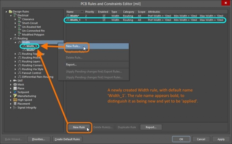
Creation of a New PCB Design Rule
Note: Keep track of the rule name for the next section. When a new rule is added, it will initially be given a default name based on the specific type of rule. If a rule with that name already exists, it will simply be given an incremented numerical suffix (i.e. Width_1, Width_2, and so on).
Modify an Existing Design Rule
1) Click on the new entry for the rule in the folder-tree pane or double-click on its entry in the summary list.
Define the new rule by setting the following values:
2) Set Name to Width_12V.
3) Define the scope of the rule by setting the first dropdown menu to Net and the second dropdown menu to 12V.
4) Set the constraints of the rule to Preferred Width = 0.50mm, Min Width = 0.50mm, and Max Width = 0.50mm.
5) Click OK.

Detailed Design Rules Control
Using the Design Rule Wizard
Design rules can also be created using the Design Rule Wizard. If you click Finish before completing the entire Wizard, the newwidth rule will be created using the system defaults for the component type you selected.
1) Launch the Design Rule Wizard from the PCB editor by clicking Design » Rule Wizard from the main menus or byclicking the Rule Wizard button in the PCB Rules and Constraints Editor dialog.
2) Choose the Rule Type.
3) Type Width_12V in the Name field and 12V Net Route Width in the Description field.
4) Select Routing » Width Constraint.
5) Click Next.

Rule Type Selection
6) Choose the Rule Scope of 1 Net.
7) Click Next.

Rule Scope Selection
8) Set the Condition Value to 12V from the dropdown and click Next.
Note: Creating a custom query is a powerful tool for the design process. Visit the Query Language Reference Page for more information on creating custom queries.

Advanced Rule Scope Selection
9) Set Rule Priority to 2 by clicking on the Width_12V and clicking Decrease Priority.

Rule Priority Selection
10) Click Next.
11) Ensure the Launch main design rules dialog box is checked and click Finish.

Rule Completion
12) Set the constraints of the rule to Preferred Width = 0.50mm, Min Width = 0.50mm, and Max Width = 0.50mm.
13) Click OK.

PCB Rules and Constraints Editor
CONFIGURING THE DESIGN RULES CHECKER
1) Open the Design Rule Checker dialog by selecting Tools » Design Rule Check.
2) Select Rules To Check » Routing.
3) Right-click in the Rules section and select Online DRC - All On.
4) Right-click in the Rules section and select Batch DRC - All On.

The Design Rule Checker dialog
INTERACTIVELY ROUTING THE BOARD
1) Confirm that the grid is appropriate for routing. To change the grid, press Ctrl+G to open the Cartesian Grid Editor, type the value 0.125mm into the Step X field, and click OK to close the dialog.
2) Check which layers are currently visible by looking at the Layer Tabs at the bottom of the workspace. If the Bottom Layer is not visible, press the L shortcut to open the Layers and Colors dialog, and enable the Bottom Layer by clicking the Eye Symbol next to the layer name.

Layers and Colors Panel
3) Click on the Bottom Layer tab at the bottom of the workspace to make it the current, or active layer, for routing.

Bottom Layer Tab
4) Select Place » Interactive Routing from the menus (shortcut: P, T), or click the Interactive Routing button on theActive Bar shown below. The cursor will change to a crosshair, indicating you are in interactive routing mode.

Interactive Route on Active Bar
5) Position the cursor over the lower pad on connector Y1. As you move the cursor close to the pad it will automatically snap to the center of the pad - this is the Snap To Object Hotspot feature pulling the cursor to the center of the nearest electrical object (configure the Range of Attraction in the Board Options dialog). Sometimes the Snap To Object Hotspot feature pulls the cursor when it is not desirable, in this situation press the Ctrl key to temporarily inhibit this feature. Left-Click or press Enter to anchor the first point of the track.

Routing Resistors
6) Move the cursor towards the bottom pad of the resistor R1, and click to place a vertical segment. Note how track segmentsare displayed in different ways (as shown in the image below). During routing, the segments are shown as:
- Solid - The segment has been placed.
- Hatched - Hatched segments are proposed but uncommitted, they will be placed when you left-click.
- Hollow - This is referred to as the look-ahead segment, it forecasts where the last proposed segment should end.

Auto-Complete Route
7) Manually route by Left-Clicking to commit track segments. For the connection that you are currently routing: Press Backspace to rip up the last-placed segment. Move your cursor back along the path; as soon as you pass over an existing uncommitted segment, the uncommitted routing unwinds back to this location.
8) Rather than routing all the way to the target pad, you can also press Ctrl + Left Click to use the Auto-Complete functionand immediately route the entire connection as illustrated here:

Auto-Complete Route
9) Continue to route all the connections on the board as shown below.

Single Layer Routed PCB
TRACE MODIFICATION AND REROUTING
Routing can use both the top and bottom layers, because the PCB was originally defined as double-sided.
1) First, delete all routing by selecting Route » Un-Route » All from the menus.
2) Now, route interactively as before. To switch routing layers press the * key on the numeric keypad to toggle between the layers while placing tracks, or use the Ctrl+Shift+Roll keys/mouse to move back and forth through the available signal layers as you route.
The PCB editor will automatically insert a via (in accordance with the Routing Via design rule) as necessary when layersare changed.
Next, modify an existing route. There are two approaches: reroute, or rearrange. When rerouting, there is no need to un- route a connection to redefine its path. Simply initiate interactive routing and start rerouting; the Loop Removal feature will automatically remove any redundant track segments.
The Loop Removal feature will automatically remove any redundant track segments, including vias. The PCB editor also includes a net analyzer that automatically analyses the route path as work progresses and removes redundant segments. Routing can start and end on the new route path at any point, swapping layers as needed.

Re-Routing Loop Removal
1) To rearrange an existing route drag the segment by clicking once to select the segment, position the mouse over the segment to display the quad-arrow cursor, then click and hold to start dragging that segment.

Dragging Existing Route
2) Note that the cursor changes if you position it over the center track vertex - this is a different mode, used to break a singlesegment into 3 segments.

Segmenting Existing Route
AUTOMATICALLY ROUTING THE BOARD
To review the ease of autorouting, complete the following steps:
1) Un-route the board by selecting Route » Un-Route » All from the menus (shortcut: U, U, A).

Un-Route PCB
2) Click the Autoroute Board icon on the Active Bar shown below. The Situs Routing Strategies dialog is split into two regions: the top region of the dialog displays the Routing Setup Report (remember to always check for warnings/errors that are shown in red), and the lower half of the dialog shows the available Routing Strategies (the selected one will be highlighted). For this board, it should default to the Default Multi Layer Board strategy.

Auto-Route Board icon on the Active Bar
3) Click on Route All in the Situs Routing Strategies dialog. The Messages panel displays the process of the autorouting.

Auto-Routed PCB
4) Do not save the auto-routed board. The tutorial will continue with the manually routed board. Press Ctrl-Z twice and see that the auto-routing and Un-Route All command can be reversed.
The auto-router will route on both the top and bottom layers, red tracks on the top layer, blue on the bottom layer. The layers that are used by the auto-router are specified in the Routing Layers design rule, which defaults to top and bottom layers. Also notice the two power net tracks running from the connector are wider, as specified by the second Width design rule you set up.
PCB DESIGN RULE VERIFICATION
1) Validate the PCB design using Tools » Design Rule Check… If there are no errors, no messages will be displayed in the Messages panel and the panel can be dismissed. The Design Rule Verification Report is created and appears a tab in the workspace.

Design Rule Check
2) The design rules for the GND net are set such that they are expected to be no more or no less than 0.50mm. Create an intentional DRC error as shown below by clicking a trace segment on the GND net, going to the Properties panel and changing the Width property to 0.4mm.

Change Width in Properties Panel
3) Rerun the Design Rule Check.
4) The rule checker should display an error in the Messages window. Dismiss the window and review the Design Rule Verification Report. The top of the report is a summary of any violations. The specific DRC violations are listed below the summary as hyperlinked text. Clicking on the link will bring the area of concern into view in the PCB editor window. Click on the one at the bottom of the report similar to the one shown below:

Clickable Error Messages
5) The error will be highlighted in a zoomed view similar to the below image. Correct the trace Width in the Properties panel or by entering Ctrl-Z to undo your width change. Save the file, and assure there are no DRC errors by rechecking again.

Route Marked with Violations
VIEWING THE PCB IN 3D
1) Switch to the 3D view by selecting View » 3D Layout Mode (shortcut: 3), or select a 3D view configuration from the list on the PCB Standard toolbar. The board will display as a 3 imensional object.
2)Zoom, using Ctrl + Right-drag mouse, or Ctrl + Roll mouse-wheel, or the PageUp / PageDown keys.
3) Pan by using a Right-drag mouse, or the standard Windows mouse-wheel controls.
4) Rotate the board using the Shift + Right-drag mouse. Note that a directional sphere appears at the current cursor position, as shown in the figure below. Rotational movement of the model is made about the center of the sphere (position the cursor before pressing Shift to position the sphere) using the following controls. Move the mouse around to highlight and select each one:
5) Right-drag sphere when the Center Dot is highlighted - rotate in any direction.
6) Right-drag sphere when the Horizontal Arrow is highlighted - rotate the view about the Y-axis.
7) Right-drag sphere when the Vertical Arrow is highlighted - rotate the view about the X-axis.
8) Right-drag sphere when the Circle Segment is highlighted - rotate the view about the Z-axis.

3D Navigation of PCB Layout
GENERATING PCB FABRICATION OUTPUT FILES
1) Create PCB Fabrication Output files by selecting File » Fabrication Outputs » Gerber X2 Files.

Generating Gerber X2 Files
2) Select Used On from the Plot Layers dropdown.

Plot Layers
3) Select Used On from the Plot Drills dropdown.

Plot Drills
4) Click OK.
The Gerber X2 file will be immediately loaded into the Altium Designer viewing tool, CAMtastic. Alternatively, batch output files can be rapidly generated, so that the PCB can be fabricated with Output Job Files. This dedicated document is a single environment for establishing all settings related to all varieties of output types including Gerber, NC drill, assembly drawings, pick and place and more. The file can also be configured for independent or combined project outputs for design variants.
CONCLUSION
You made it to the end of the PCB design tutorial! Thank you for your attention. The PCB design tutorial provided just a quick overview into the design process with Altium Designer. Check out other Getting Started guides for insight into using robust features like Draftsman® and ActiveRoute®.
Remember to visit Altium.com/documentation to find other useful documentation, and read the article Exploring Altium Designer for an explanation of the interface, information on how to use panels, and guidelines for managing design documents. If you want a more in-depth training experience, visit our Events page.
