








High-Speed Signal Routing: The 10 Important PCB Design Constraints

At a Glance
Your high-speed signal routing strategy takes attention to restraints and creative floor planning. Here’s how to route high-speed signals the right way.


Your modern digital PCB is most likely acting as a high-speed digital system, regardless of whether you intended for this to be the case. Of course, the impact and the level of evaluation required depend on the rise time of your signals, and this will often constrain how and where you route certain signals on the PCB. These constraints can be defined as PCB design rules in your PCB project, and this article will run over some of the common constraints imposed in high-speed designs to ensure successful routing.
10 Important High-Speed PCB Routing Constraints
Trace Width Values by Layer
The standard interfaces used to transfer high-speed digital data are all impedance-controlled interfaces. The driver connected to a trace expects the trace to have a specific impedance value, and your ECAD software must maintain this when you begin routing. Similarly, receivers are terminated to a specific input impedance or load capacitance and only function as specified based on the impedance of the connected trace.
Once you have an impedance model established for your design, the trace width constraint and allowed variations should be established for each signal layer and then applied to various net classes. This requires a calculation of the trace impedance in different geometries.
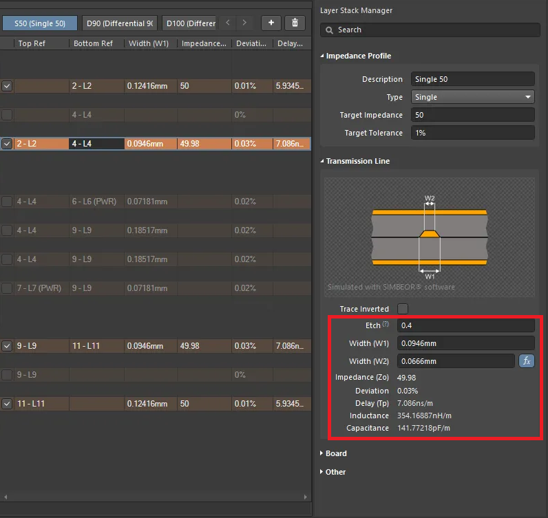
In Altium Designer, transmission line impedance calculations are performed in the same tool that is used to define the PCB layer stack.
- Open Design » Layer Stack Manager and configure the stackup, including copper thicknesses, dielectric thicknesses, and dielectric material properties.
- Select the Impedance tab and click Add Impedance Profile, or the add button if a profile already exists.
- In the Properties panel, select the profile type and enter the Target Impedance and Target Tolerance.
- Enable the signal layers that will use this profile, then assign the reference layers in the Top Ref and Bottom Ref columns.
- Select each enabled signal layer and review the calculated trace width. For a differential profile, lock either Width or Trace Gap so the solver calculates the other value for the target impedance.
- Save the layer stack. The resulting profile can then be selected in the applicable Width or Differential Pairs Routing rule.
Impedance-Controlled Net Classes
To ensure the routing is maintained at the correct impedance on specific interfaces, we use a simple process of grouping nets and creating net-specific design rules to enforce the trace width. Grouping nets with the same impedance into net classes is the fastest way to apply multiple constraints to net groups, and this includes the major high-speed constraints such as trace width and matched propagation delays in parallel buses and differential pairs.
- In the schematic, attach a Net Class directive to each net that belongs to the group and enter the same class name for each directive. A blanket with an attached parameter set can also group multiple nets.
- Open Project » Project Options » Class Generation and enable the generation of user-defined net classes. Update the PCB and execute the class-related changes in the Engineering Change Order.
- Alternatively, create the class directly in the PCB editor through Design » Classes. Add a new class under Net Classes, name it, and move the required nets from Non-Members to Members.
- Open Design » Rules and create the required rule, such as Routing » Width.
- Set the rule scope to InNetClass('ClassName'), replacing ClassName with the actual class name.
- Configure the constraints. For controlled impedance routing, enable Use Impedance Profile and select the profile created in the Layer Stack Manager.
- Give the class-specific rule higher priority than broader rules of the same type, then apply the changes.
What about the impedance variation? How should you account for this if you plan to change trace width? It is possible to do this by using neck-down, i.e., changing the trace width as the trace enters a room, for example, in a BGA footprint. If you can anticipate these routing needs, then plan to account for the change in trace width within your PCB design rules.
Return Path Confinement
Return path confinement checks verify that a trace does not cross a reference plane boundary, such as the gap between two rails in a power layer. Crossing this gap interrupts the nearby return path and forces return current to detour. In Altium Designer, a Return Path rule uses the assigned impedance profile to identify reference layers and check copper continuity beneath the routing.

Timing Skew
Skew between signals in parallel buses or within a differential pair needs to be minimized when delay matching requirements are very strict. There are three categories of timing skew that need to be constrained in a PCB layout:
- Signal delay matching within a differential pair
- Delay matching between multiple differential pairs
- Length matching in mixed buses (single-ended and differential pairs)
This is why we like to define net classes; it makes timing constraints much simpler, as they can be implemented for all nets in that net class.
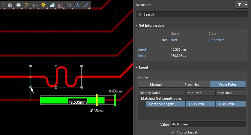
For interfaces like PCIe and DDR, the timing constraints are so tight that the pin-package propagation delay is needed to accurately ensure signals reach their destination within the required time window. Information can be supplied by the component vendor in order to model the high-speed interface in question. When you create a schematic symbol for the library component, the pin delay information can be incorporated into the pin definitions at each end of the link, and these delay values will be incorporated in the delay tuning tool during routing.
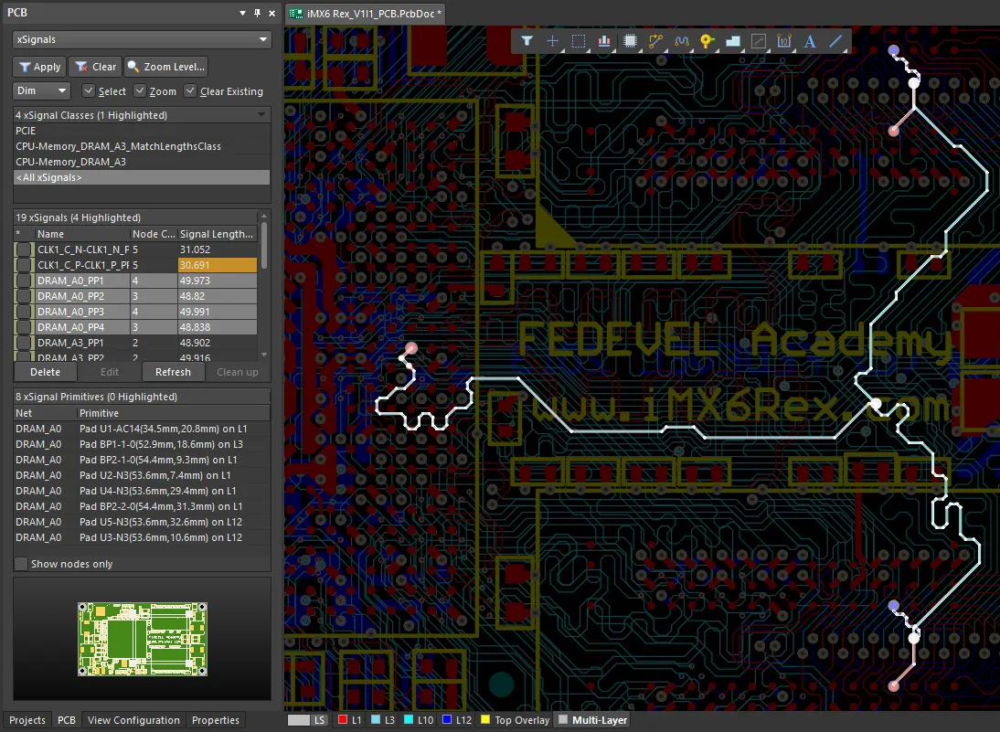
To include pin-package delays in the delay tuning calculation during routing in Altium Designer, nets in the interface in question need to be included in xSignals. This tool accounts for all delays from point to point between two integrated circuits, and these are used within the delay tuning calculation.
Routing Layer Confinements
In high-layer-count boards, it is often the case that certain net classes or differential pair classes are assigned only to specific layers. There are two major reasons for doing this:
- Different layers are separated based on impedance, aiding controlled impedance testing
- Some routes require more spacing to ensure low crosstalk, leaving little room for other signal routes
For example, it is common to separate different interfaces such as DDR, 90 Ohm differential pairs (e.g., USB), 100 Ohm differential pairs, and other impedance-controlled buses onto their own layers with common pair design. This separation can also be done by trace width/spacing value, as it helps manufacturers more easily swap out equivalent materials when necessary.
A Routing Layers rule specifies which signal layers can be used by the targeted net class or differential pair class. Class-specific rules allow each interface to use its assigned layers while retaining a broader rule for other routing.
- Open Design » Rules and create a new rule under Routing » Routing Layers.
- Set the custom scope to InNetClass('ClassName') for a net class or InDifferentialPairClass('PairClass') for a differential pair class.
- In the layer list, enable Allow Routing for the permitted layers and disable it for the remaining layers.
- Give this rule higher priority than any broader Routing Layers rule that targets the same nets.
- Apply the rule and run a design rule check to identify existing routing on prohibited layers.
Clearances to All Other Objects by Layer
Clearance values are normally different for internal vs. external layers due to the outer-layer plating process. However, because many high-speed designs also tend to be high-density designs, it’s common for different internal layers to require different clearance values. This arises due to the use of sub-laminations, which require an additional plating process and build up to a higher plated copper thickness than the base foil weight.
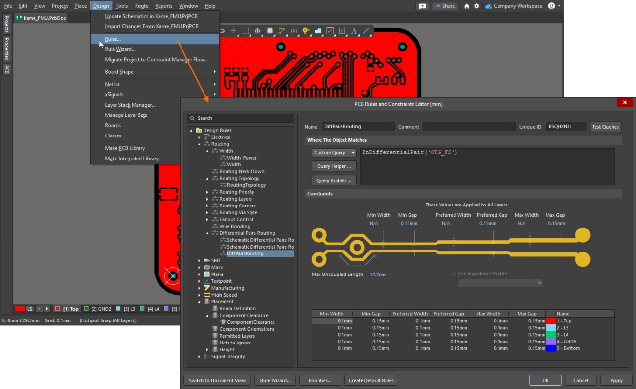
In Altium Designer, the clearances by layer can be defined using the query system:
- Open Design » Classes in the PCB editor and create a new layer class under Layer Classes.
- Name the class and add the layers that share the same clearance requirements. Repeat this for each group requiring a different clearance.
- Open Design » Rules and create a new rule under Electrical » Clearance for each layer or layer class.
- Select a custom query for the first object scope. Use OnLayer('Top Layer') for an individual layer or InLayerClass('LayerClass') for a layer class, substituting the actual layer or class name.
- Set the second object scope to All so the rule checks clearance to other copper objects on the applicable layer.
- Select Different Nets Only and enter the required minimum clearance. Use the clearance matrix if different object combinations require different values.
- Give the layer-specific rules higher priority than the general clearance rule, apply the changes, and run a design rule check.
Make sure to get the clearance requirements by copper weight (internal and external) from your PCB fabrication services provider.
It is also possible to define clearances by layer using the new Constraint Manager. This gives a matrix-based approach for clearance definitions, which designers of other ECAD software will find much more familiar. Learn more about the Constraint Manager in the video below:
Net-Specific Via Sizes or Templates
I’ve discussed elsewhere on the Altium blog how via impedance works and at what frequencies vias need to be designed to a specific input impedance. These via sizes and anti-pad sizes will be net-specific for a particular stackup and layer span, and the restriction on via/pad size can be defined using PCB design rules.
Via sizes can be constrained in two ways:
- By defining the allowed sizes for specific nets/net classes
- By assigning a via template to specific nets/net classes
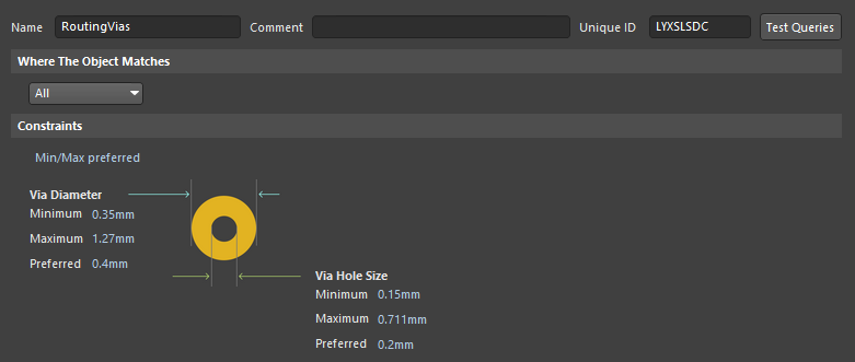
Determining the right via size is not as simple as using an online calculator to determine via sizes. It requires a 3D electromagnetic field simulation, or at least an empirical model developed from simulation data. Once the via sizes and anti-pad sizes are determined, enforce these as design rules to ensure the important high-speed nets are constrained to the right via sizes.
Via Anti-Pad
The via anti-pad is another part of designing to via impedance, as the clearance to the plane adjusts the capacitance along the via barrel. In all designs, there will already be a minimum clearance requirement between via pads and the nearby copper on plane rails or large power rails. The via-to-copper clearance value can be adjusted on specific nets using a PCB design rule on a net or net class basis.
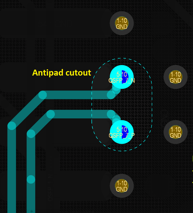
For differential nets, the anti-pad shape may be oblong or elliptical, rather than circular around individual vias. This shared anti-pad is best defined by drawing the anti-pad shape, either as a plane cutout or polygon cutout. An example is shown below.
Via-in-Pad Allowance
One quality of modern high-speed PCBs is that they tend to also be high-density PCBs. This is because most processors now come packaged in BGA packages, and at low pitch, this will require via-in-pad to complete fanout routing. Even with coarse-pitch BGA packages using dog-bone fanout, the optimal placement of bypass caps is on the back side of the BGA using via-in-pad.
By default, ECAD software checks for via-in-pad and will flag it as a DRC violation if present. However, via-in-pad can be allowed within the design rules to support BGA fanout routing.
Open Design » Rules and create a High Speed » Via Under SMD rule. Enable Allow Vias under SMD Pads and scope the rule to the intended pads, using IsPad AND WithinRoom('BGA_Fanout') for a defined fanout room. Give it higher priority than the general rule. Also configure a matching Same Net Only Clearance rule with zero SMD pad-to-via and pad-to-via-hole clearance for the approved vias.
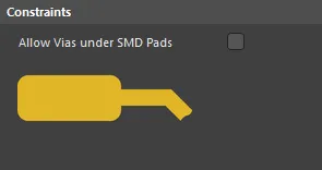
Make sure to specify the relevant vias as filled and capped using the IPC-4761 via types option in the Properties panel. This can also be done by manually selecting the specific via group to be plated and capped, or by adding a fabrication note to your master drawing if all vias are to be filled and capped.
Differential Pair Uncoupled Length
The uncoupled length of a differential pair will contribute to the return loss in a differential channel, and so it’s important to determine an appropriate uncoupled length in some applications. The uncoupled region will most often arise when routing out of a dense pin field in a BGA, where the traces need to separate from each other in order to route around vias.
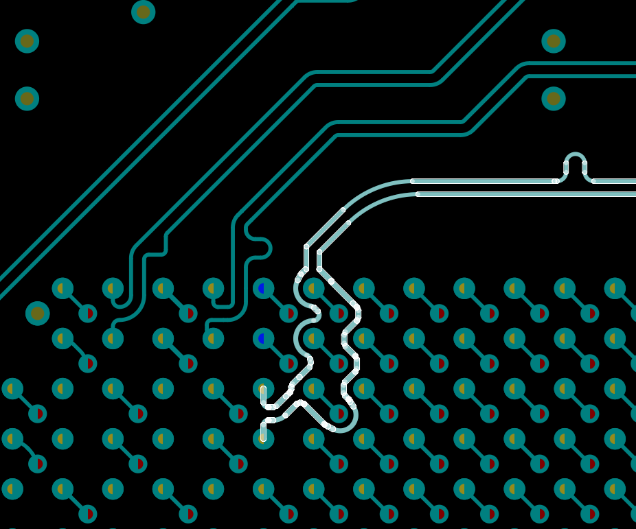
Calculating the uncoupled length is not a simple calculation, as it relies on a proper critical length calculation based on your channel bandwidth. A decent strategy is, if you know that your differential pairs will have an uncoupled region in the fanout routing, to start by designing the pair with loose coupling, because this will reduce the impedance mismatch at the uncoupled region and reduce mode conversion.
To learn more about the PCB design rules system in Altium Designer, watch the video below.
Whether you need to build reliable power electronics or advanced digital systems, use Altium’s complete set of PCB design features and world-class CAD tools. Altium provides the world’s premier electronic product development platform, complete with the industry’s best PCB design tools and cross-disciplinary collaboration features for advanced design teams. Contact an expert at Altium today!
Frequently Asked Questions
How can I check whether PCB traces cross gaps in their reference planes?
In Altium Designer, create a High Speed » Return Path rule scoped to the relevant nets or net class. Select the impedance profile that defines their reference layers, configure the minimum distance from the trace to reference copper boundaries, and run a batch design rule check. The check identifies routing over reference copper discontinuities, including gaps between power rails.
How do I restrict a net class or differential pair class to specific routing layers?
Create a Routing » Routing Layers rule in Design » Rules and scope it with InNetClass('ClassName') or InDifferentialPairClass('PairClass'). Enable Allow Routing only for the permitted signal layers, then give the rule higher priority than broader Routing Layers rules. These settings constrain routing and allow design rule checks to identify existing traces on prohibited layers.
How do I assign via sizes or via templates to specific nets and net classes?
Create a Routing » Routing Via Style rule and scope it to the target net or net class using InNet('NetName') or InNetClass('ClassName'). Define the minimum, preferred, and maximum via diameter and hole size, or configure the rule to use approved via templates. Give the rule higher priority than the general via rule. Via layer spans are defined separately in the Layer Stack Manager.
How do I create net classes and assign high-speed PCB routing rules?
Net classes can be created with schematic Net Class directives or directly through Design » Classes in the PCB editor. For schematic-defined classes, enable user-defined net class generation in Project Options and transfer the changes to the PCB. In Design » Rules, scope each applicable routing or timing rule with InNetClass('ClassName'), configure its constraints, and give it priority over broader rules of the same type.

About Author
Related Resources
Related Technical Documentation
Table of Contents
- 10 Important High-Speed PCB Routing Constraints
- Trace Width Values by Layer
- Impedance-Controlled Net Classes
- Return Path Confinement
- Timing Skew
- Routing Layer Confinements
- Clearances to All Other Objects by Layer
- Net-Specific Via Sizes or Templates
- Via Anti-Pad
- Via-in-Pad Allowance
- Differential Pair Uncoupled Length
- Frequently Asked Questions
Deliver Faster with a Unified PCB Design Platform
- Find tools for every PCB challenge
- Route faster with precision and control
- Enjoy smarter sourcing for reliable manufacturing
- Simplify electronics design review Wwrkflow
Learn More
Thank you, you are now subscribed to updates.



