


Transition from Hobbyist PCB Manufacturer to Professional Designer with Altium


Most new designers start off with freeware when they need to create their first PCB designs, but free PCB design software lacks many features required to create real circuit boards. Hobbyist PCB designers and makers need a range of tools to create high-quality circuit boards and eventually create real devices. Instead of using free PCB layout software and other programs to help get designs into production, hobbyist PCB makers need professional design tools to build professional hardware.
Altium Designer is an excellent choice for hobbyist PCB designers who want to get a circuit board up to production grade. The PCB layout, routing, and production preparation tools are ideal for creating professional hardware, and for guiding makers along the path to becoming professional designers. Here’s what new designers and makers can expect from Altium Designer and how its rules-driven engine helps them build the best designs.
ALTIUM DESIGNER
The only PCB design package with a complete set of features for both hobbyist PCB designers and experienced professionals.
Your very first PCB design application is probably a freeware platform, but it doesn’t have to stay that way. Hobbyist PCB designers and makers often start with a small budget and they need an easy-to-use toolset to get started on new designs. Eventually, as designs get more complex, a free PCB design software application won’t do the job, and a more advanced platform is needed.
Altium Designer was made for PCB designers of all experience levels, including industry veterans and brand new designers. The complete set of PCB design tools in Altium Designer can help guide hobbyists and makers through the complicated world of PCB design and into full-scale production with a complete toolset. If you’re an experienced designer or you’re a hobbyist PCB maker that wants more skills, Altium Designer gives you the features you need in an easy-to-use interface.
Getting Started With Schematic Design
All PCBs start from electronics schematics, and even free PCB design programs need to have some schematic design and viewing capabilities. Some free PCB design programs only do PCB layout and routing, forcing a designer to find a compatible circuit design program. Altium Designer eliminates the need to find multiple compatible programs, instead allowing designers to create a complete set of schematics in the same program they’ll use for their PCB layout.
So what does it take to create professional schematics? Whether you’re a maker or experienced designer, your schematic design tools should include some of the following features:
- Access to component libraries and automated creation of a BOM
- Placement of ports, net directives, and parameter sets
- An integrated SPICE simulator for evaluating circuit functionality
- CAD tools for creating custom schematic symbols for new components
- Instant schematic capture into a new PCB layout and integration with manufacturing tools
This is just the beginning of the various tools hobbyist PCB designers need to keep their designs at the cutting edge.
Advanced Tools for Schematic Design
Today’s advanced designs can get very complex, and they can involve multiple boards, multiple circuit blocks, and a range of capabilities that can’t fit into a single schematic. Altium Designer goes beyond free PCB design software and helps designers create a schematic hierarchy for their new design. Altium Designer is also the best multi-board PCB design system and includes tools specifically for organizing boards into multiple sections. You won’t be able to create these types of advanced designs in free PCB design software applications.
- Basic schematic structures are flat, while advanced designs will often use a hierarchical structure to stay organized.
Learn more about the difference between flat and hierarchical schematics.
- When you’re working in an individual schematic sheet, complex circuits can be difficult to keep organized. Altium Designer’s CAD tools make organization easy.
Learn more about keeping your schematic sheets and circuits organized.
- Getting started with a new schematic is easy in Altium Designer. A single process can be used for design of simple or complex circuits.
Learn more about getting started with a new schematic in Altium Designer.

Hierarchical schematic design features go beyond hobbyist PCB design software and help you keep advanced designs organized.
From Schematic Editor to a New PCB Layout
When you’ve finished designing schematics, it’s time to turn them into a new PCB layout. Every new circuit board will begin with schematic capture into a blank PCB layout, and components are subsequently placed around the PCB. A set of CAD tools is needed alongside some simple data management tools to keep schematics, PCB layouts, and component libraries synchronized.
While free hobbyist PCB design programs still separate these features into different programs, Altium Designer helps you stay more efficient by keeping schematic capture and PCB layout functions in the same program. In addition, PCB layout data and schematic data stay synchronized thanks to the unified data model in Altium Designer’s underlying PCB design engine. Designers won’t need to switch back and forth between different programs; they can start upgrading hobby PCB designs or create advanced layouts with a complete set of PCB layout and routing features.
Hobby PCBs Will Benefit From Advanced Layout and Routing Tools
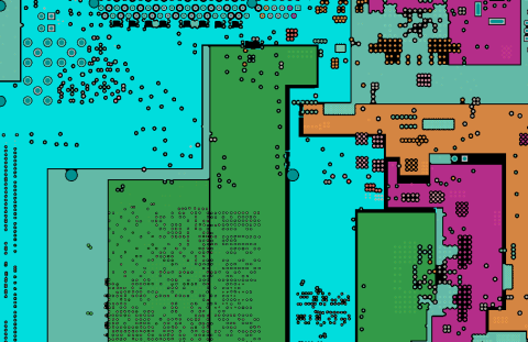
Every circuit board will get created in a PCB layout, which takes a complete set of CAD tools and routing features. Once you capture your schematics and import them into a new PCB layout, Altium Designer’s routing features are instantly accessible and can be used to implement any routing topology. Forget about using the autorouter in hobbyist PCB design software, take full control of your PCB layout and routing with advanced interactive tools in Altium Designer.
- Every PCB design begins as a blank PCB layout after importing components from schematics. Altium Designer makes this process simple without using multiple programs.
Learn more about capturing your schematics as a PCB layout in Altium Designer.
- Hobbyist PCB software won’t give designers the control they need over routing tools. Instead, interactive routing tools give you control over routing path, spacing, width, impedance, and much more.
- Layout and routing are fundamental that go together. Altium Designer gives you a complete toolset for routing and PCB layout in an integrated design environment.
Learn some layout and routing tips for hobby PCBs and advanced designs in Altium Designer.

Altium Designer helps you stay organized by linking your schematics and PCB layout into a unified design environment.
Altium Designer as a Hobbyist PCB Design Software
Whether you’re working on a hobby PCB project or you need to produce 1 million units of your next design, Altium Designer has the complete set of design features every designer needs. Altium Designer is more than a circuit diagram editor or circuit board layout utility, it’s a unified rules-driven PCB design platform that helps you go from concept to product in a single program.
With organization and data management tools, designers can enforce a design hierarchy and access a complete set of PCB layout utilities in a single program. When you’re ready to send your circuit board out for manufacturing, your design data and your project structure will be copied into your deliverables and checked against your design rules. These features are meant to help every designer become a seasoned professional and create advanced circuit boards.
Altium Designer’s Rules-Driven Engine Helps You Stay at the Cutting Edge
The secret to Altium Designer’s tool integration and powerful design interface is its rules-driven design engine. This underlying design environment links your tools together to ensure every aspect of your board can be checked against important design rules. For hobby PCB projects that need to be put into production, design rules help you spot design errors that prevent manufacturing. Thanks to Altium Designer’s rules engine and a complete toolset, hobbyist PCB designers can create more advanced designs and get their boards up to production grade.
- Altium Designer’s rules-driven design engine helps every designer comply with industry standards and application-specific design rules. Designers can also create custom design rules and run DRCs anytime during design.
See what makes Altium Designer different from other platforms.
- Rules-driven PCB design is all about integration, where multiple PCB design features are present in a single program and obey a single set of design rules.
Learn more about the rules-driven design interface in Altium Designer.
- After you’ve completed your new design and verified your PCB layout, you can instantly share your design data with your collaborators or a manufacturer using the Altium 365 platform.
Learn more about sharing your PCB design data with the Altium 365 platform.

Altium Designer’s complete set of PCB design tools helps any designer build advanced electronics.
Whether you’re a hobbyist PCB designer or a seasoned professional, Altium Designer has something for everyone. The unified design environment provides everything designers need to create advanced electronics and get them through manufacturing. Stay at the cutting edge and at your most productive with the powerful PCB design tools in Altium Designer.
There are various licensing options for Altium Designer, but you may also contact us for other license types that may be more suitable for a hobbyist PCB designer.
We have only scratched the surface of what is possible to do with Altium Designer on Altium 365. You can check the product page for a more in-depth feature description or one of the On-Demand Webinars.

About Author
Related Resources
Related Technical Documentation
Table of Contents
Design to Release, Without the Friction
- Keep reviews tied to the right version
- Reduce handoff confusion and rework
- Spot sourcing and release risk earlier
- Work solo, share when needed
Get Started
Thank you, you are now subscribed to updates.


