


How to Place PCB Cavities for Embedded SMD Parts

At a Glance
Embedded cavities can be used to place SMD parts, internal copper fills for heat sinking, or as a highly shielded edge-plated region.


When we talk about embedded, we aren’t always talking about embedded software. Components can also be embedded in a PCB by placing a cavity region in the internal layers. Cavity regions in a PCB allow component placement, filling with copper for an embedded heatsink, or inset placement below a surface layer in a PCB. If you want to free up space on surface layers, or just lower the profile of your PCBA, cavities are one option that could help.
Types of Embedded Cavities in IPC Standards
The newest revision of the IPC standards for rigid PCBs defines three types of embedded cavities and their acceptability criteria. The following cavity types are defined in IPC-6012F:
|
|
|
|
|
|
|
|
|
Cavities can have copper internally, such as traces and pads, making them Type 2. If there is also some plating along the wall, such as partially plated walls, then this would be a Type 3 cavity.
Cavities can also be totally filled with copper, sometimes referred to as a copper coin (or “coining”). This is normally done so that the region internal to the PCB can act like a large heat sink; when placed under a component, it will provide significant heat transfer to the interior of the board. If the coin is then connected to a plane or placed near a large plane, it will provide significant heat transfer away from a hot component. This can also be used with bonding the assembly to the enclosure, so that now the coin + enclosure together will form a large heat sink.
SMD Components in Cavities Using PCB Footprints
Although coining is an excellent use case, the typical method is to use a cavity to hold SMD components internally. This would involve defining some pads in an internal layer for an SMD component. Typically you would route into these pads in the same layer coming from outside the cavity walls, so this would be a Type 2 cavity.
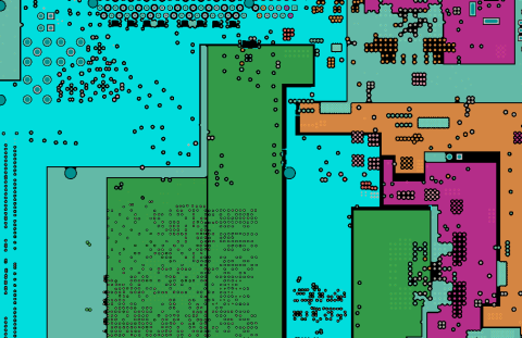
A variation on this is to have an inset cavity, which is cut into one of the surface layers. This type of cavity is probably most common and is used to reduce the overall z-axis height of the board. An example image showing SMD components in a Type 2 inset cavity is shown below.

In order to define a cavity for an SMD part in Altium Designer:
- Define a cavity region in the PCB footprint
- Place the footprint on an internal layer in the PCB layout, and then draw the cavity manually
Option 2 is useful because it allows you to embed any component in your libraries without modifying footprints. However, Option 1 is also useful because it shows a more realistic view of the cavity cutout in 3D.
Option 1: This is done by drawing out a solid region in the PCB footprint and setting its Type of "Cavity" in the properties panel. It is typically recommended to match the cavity region size to your component courtyard (at minimum) plus some additional allowance for fabrication tolerances (see below). This will ensure there will be enough room to place the cavity during pick-and-place as this will account for clearances to the cavity walls around the component pads.
An example for an nRF52 MCU in WLCSP with a BGA footprint is shown below. The Cavity region is drawn around the edge of the package and is expanded around the courtyard to account for the routing tool diameter. Note that, if you intend to place the part in a cavity, it may be required to remove the silkscreen layer or expand the silkscreen so that it sits outside the edge of the cavity. Due to the difficulty in placing silkscreen around a cavity edge when the cavity is not yet defined in the PCB layout, I would suggest to eliminate the silkscreen in the footprint and draw it out manually, or just place it outside the cavity edge.

Once the footprint is imported into the PCB layout, the component can be selected and placed into an internal layer using the properties panel. Note that the cavity has a Height attribute that is defined in the PCB footprint; the height will define how deep the cavity will be into the depth of the board order to hold the component. You can then export the Cavity definition in your Gerbers and include it in your fabrication drawing as normal. Make sure to match the placement in the internal layer to your copper orientation in the PCB stackup!
To learn more about using cavity regions, read the documentation at the link below.
Option 2: Note that a Cavity region is not required to place components into an internal layer, you can always draw out the cavity by hand in a mechanical layer in the PCB layout without placing it into a PCB footprint (see below). To embed a component without using a Cavity region in the PCB footprint, you can just select the component and change its Layer property to your desired inner layer.
Once you do this, the pads for that component will be placed into the internal layer as normal. However, this option does not create a cavity view in 3D, even if you add the cavity outline manually using a mechanical layer. Instead, the 3D body is just shown being dropped into the substrate slightly; if dropped too much the component will not appear at all, so it is obviously not an accurate representation of the embedding. However, I am able to do this without any modification to the footprint; I just need to place the cavity outline and polygon cutout with clearance in the layout manually.

Which is the best option to use? Personally, I prefer Option 2 if I need to do something with a cavity because I prefer to not have to draw out the cavity in my footprints. Also, if the layer stack changes, I might be required to also change the Cavity height in the footprint, and it just adds another layer of work and verification. Finally, it's equally easy to configure the copper pullback around the cavity edge with either method; Option 1 just uses a clearance rule (Object to Region), while Option 2 uses polygon clearance and/or keepouts.
However, if you need to have 3D verification of the cavity region in your PCB due to mechanical constraints, or you have a single component that you will only ever use in a cavity, then Option 1 is superior.
Manually Drawing Cavities in Your PCB Layout
If you want to manually draw out a cavity in your design, even without defining a region, you can do it with a mechanical layer in the PCB layout.
To get started, you first need to select a routing tool radius and use this to set the corner radius of your cavity outline. Draw the outline in a new mechanical layer in your PCB Editor. You can use arcs, or a rectangular region with an applied corner radius. Name the mechanical layer something recognizable, like “CavityLayer”.

Once the cavity outline is drawn and the appropriate radius is applied, you need to apply clearances around that outline (see below). From this outline, you could use a keepout to prevent anything from appearing in the cavity region (basic Type 1 cavity). If you are clearing copper pour from inside the cavity, you could use a polygon cutout region and size it larger than the cavity outline to account for clearance and routing tolerance.

There are four design rules to follow regarding cavities:
- Clearances: Make sure to treat the outline of a cavity like a board cutout regarding clearances and tolerances.
- Routing: You can route above/beneath the cavity region on other layers, but only blind/buried vias can be used in the cavity region.
- Keepouts: Placing keepouts in the cavity region that matches the cavity boundary. If you are using an inset cavity, a keepout will be required on the surface layer.
- Edge plating: If you’re designing a Type 3 cavity, or Type 2 with edge plating, apply a negative clearance around the cavity edge.
Fabrication Notes for Cavities
If you followed the advice above and placed your cavity in a mechanical layer, you can also export that cavity definition into standard fabrication data (Gerbers or ODB++). When you create your outputs, make sure to include the mechanical layer for your cavity in your Gerber export.
Once the cavity is defined in your design, make sure to include a fabrication note that clearly states the fabrication needs for the cavity. When writing the fabrication note, make sure to include the following information:
- The starting and ending layers for the cavity (L2 and L3 in my example)
- The Gerber file containing the cavity routing path
- The routing tool radius
- The required tolerance on the routing path (usually +/- 10 mils)
- The cavity Type as defined in the IPC-6012F standard
Because your fabricator generally won’t look at your native board files, it’s important to clearly specify this data in your fabrication documentation. If there is an option to include special notes on your quote form, make sure to copy the fabrication note there too.
Whenever you need to place special mechanical features into a PCB layout, you can create industry-standard documentation for your PCB with the OutJob File feature and the world-class CAD tools in Altium Designer®. To implement collaboration in today’s cross-disciplinary environment, innovative companies are using the Altium 365™ platform to easily share design data and put projects into manufacturing.
We have only scratched the surface of what’s possible with Altium Designer on Altium 365. Start your free trial of Altium Designer + Altium 365 today.

About Author
Related Resources
Related Technical Documentation
Table of Contents
Design to Release, Without the Friction
- Keep reviews tied to the right version
- Reduce handoff confusion and rework
- Spot sourcing and release risk earlier
- Work solo, share when needed
Get Started
Thank you, you are now subscribed to updates.

