Getting Your Layer Stack Done Right the First Time

Failure to properly design the layer stack is a common mistake in PCB assembly. This blunder often occurs during the final stages of fabrication, but can easily be prevented by including the appropriate features in the beginning stages of PCB design. Read on to learn about what layer stackup features you’ll want to include in your design.
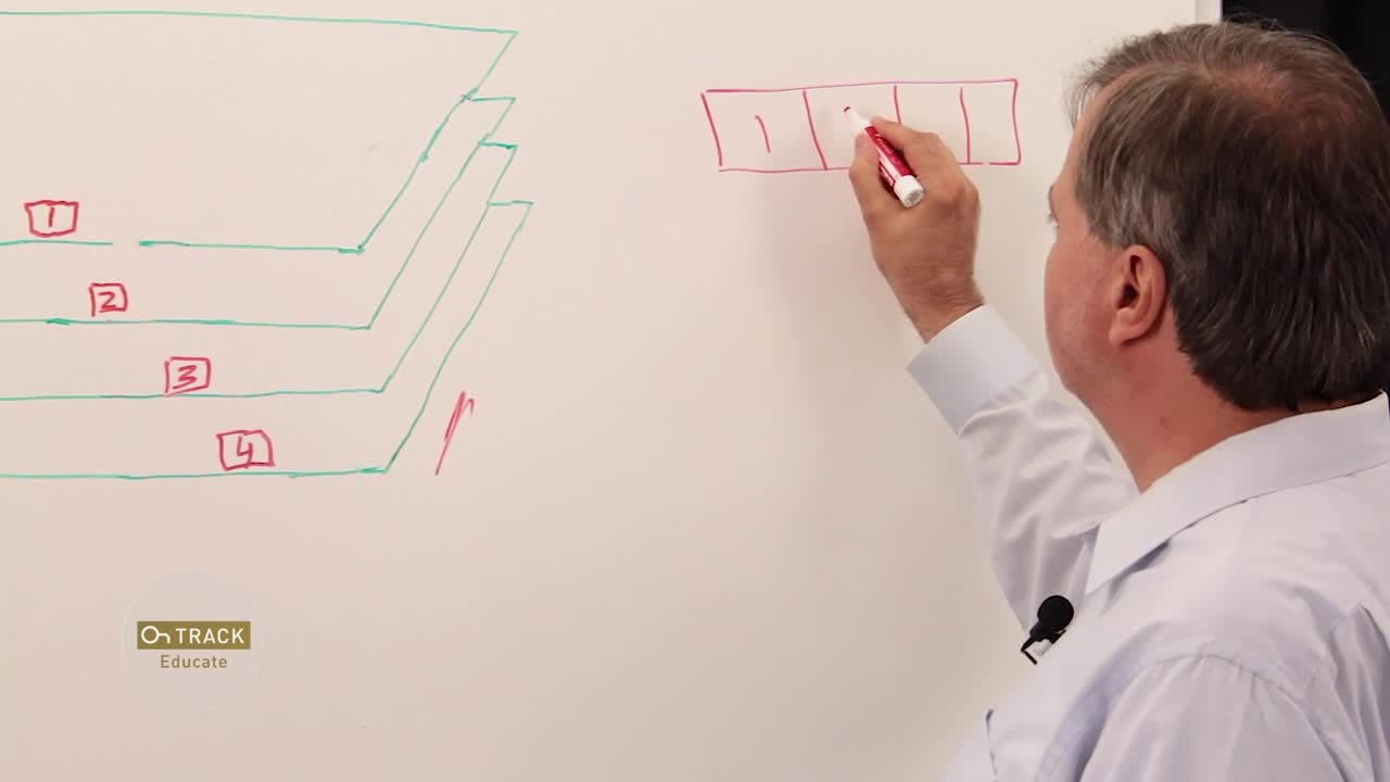
One of the most common mistakes during the PCB fabrication process is improper layer order. If left unchecked, it can cause an entire design process to fail. The PCB assembly process may function from an electrical continuity standpoint. It may even pass an electrical inspection. However, in designs where the order of plane to signal layers and the proximity of layers with respect to each other is paramount, failures will occur at the final functional assembly level. How can we prevent this from happening?

Layer Stacks: It’s All About the Details
In order to guarantee that the fabricator has the required information to order the layers properly and perform a post-process visual inspection, details must be engineered directly into the copper geometry. It is the responsibility of the PCB designer to include these features in the design to provide a mechanism for the inspection of the final assembly. These features include:
-
Accurately identifying layers with a defined numbering scheme in relation to all other layers.
-
Adding stacking stripes to facilitate easy visual inspection of the layer order.
-
Providing test traces that allow for easy verification of post-etch copper thickness and width.
Designing the proper copper features into the fabrication data provides a high degree of confidence that the proper layer stackup order will be achieved. By providing these details early on, you can streamline the manufacturing process by preventing issues, reducing costs, and saving time.

Want to learn how to add the features you need to get your layer stack done right the first time? Download our free whitepaper about Getting the Layer Stack Right.

About Author
About Author
Chris earned his Bachelor of Science degree in Electrical and Electronics Engineering from Oregon State University in 1993, and has worked as a design engineer in the Bio-Medical, Industrial Controls, Motor Drive, and Defense industries. His experience ranges from concept through research, development, design, documentation, manufacturing, application engineering, and support. He joined Altium in 2007 and brought with him his background in power electronics, data acquisition, and controls.
Related Resources
Related Technical Documentation
Table of Contents
Design to Release, Without the Friction
- Keep reviews tied to the right version
- Reduce handoff confusion and rework
- Spot sourcing and release risk earlier
- Work solo, share when needed
Get Started

PCB Design
Equip engineers with everything needed to design modern, high-performance PCBs.

Product Design
Combine advanced PCB design with cloud-based collaboration to streamline development.

PCB Manufacturing Handoff Tools
Faster design-to-production handoff with your contract manufacturer.

Manufacturing Made Easy
Centralize DFM reviews and packages to accelerate PCB production handoff.


