






Use a PCB Gerber Viewer to Inspect Your Fab Files in Altium 365

At a Glance
A PCB Gerber viewer can help you inspect your board as you prepare for manufacturing. Use the features in Altium 365 to compare and share your Gerber files.


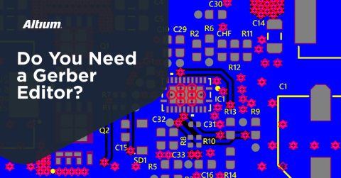
A PCB can pass its native design rules and still reach fabrication with an incomplete or incorrect manufacturing package. An omitted copper layer, incorrect drill export, or unintended solder mask opening can survive because the problem occurs in output generation rather than routing. A PCB Gerber viewer gives engineers a way to inspect the exported geometry that will enter the fabricator’s CAM review process.
Manufacturing file reviews should be performed as one of the final steps before a design receives signoff and can be put into production. A useful review combines layer inspection, dimensional checks, connectivity verification where available, and confirmation that the drawings and manufacturing files describe the same revision.
Layer by Layer Gerber Inspection
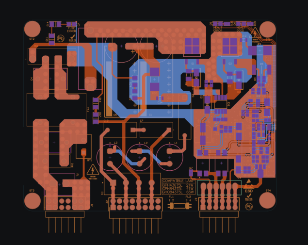
The PCB layout is normally the document which gets reviewed as it contains much more information than would be exported into a manufacturing file package. The Gerber file export only includes merged images for each layer, and the entire point of these file exports is so the fabrication house can program the imaging, etching, drilling, plating and continuity testing processes. Because almost all design teams do not have access to proper CAM software normally used for process planning, they need to use the viewer or CAM capabilities in their PCB design software to pass the final review gate.
CAM software and Gerber viewers have their peculiarities. First, each layer should be viewed individually, followed by selected overlays that expose relationships between copper, hole locations/diameters, mask openings, and silkscreen markings. Enabling every layer simultaneously can hide small defects beneath overlapping features. Measurements are useful wherever acceptance depends on a minimum width or clearance; the screen’s appearance at a convenient zoom level provides no dimensional assurance.
A focused review covers these recurring problems:
- Copper layers: narrow necks, unintended bridges, isolated copper, and clearances below the agreed manufacturing limits.
- Plane layers: missing connections, incorrect clearances around holes, and thermal relief geometry inconsistent with the intended connection.
- Drill overlays: use to identify duplicate or overlapping drill hits, holes encroaching on unrelated copper, and annular ring sizes
- Solder mask: unintended exposed copper, covered soldering surfaces, and narrow mask webs between adjacent openings.
- Paste layers: missing apertures, unintended apertures, and incorrect reductions or segmentation for the planned stencil.
- Silkscreen: markings over exposed pads, unclear polarity indicators, incorrect cutouts, and inadequate copper clearance to routed edges.
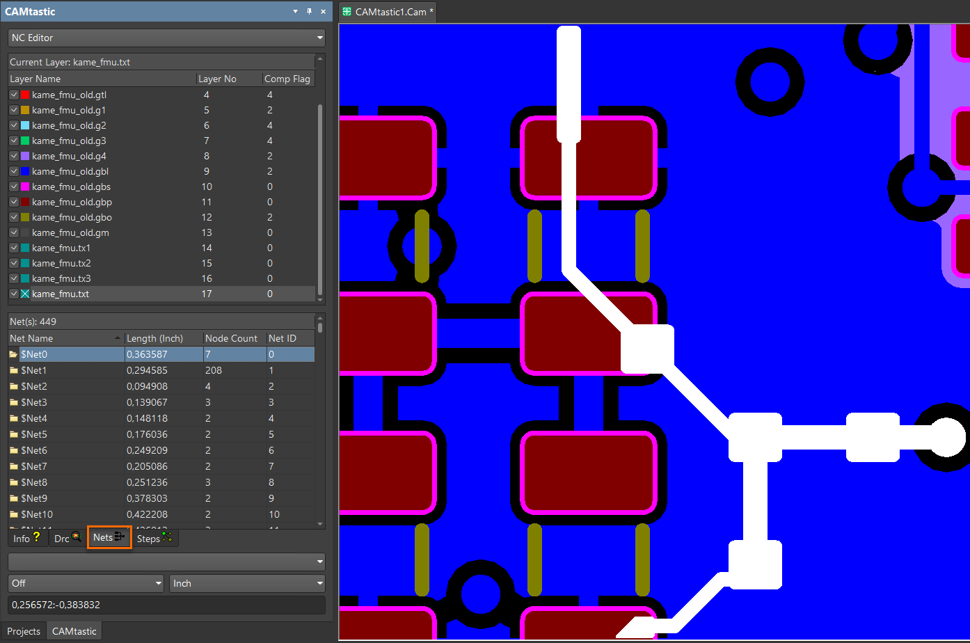
For Altium Designer users, CAMtastic supports manufacturing checks for annular ring, trace width, copper spacing, solder bridging, and shorts. Its tolerances should reflect the supplier’s requirements rather than remain at generic defaults. Visual review then adds judgment about whether the exported geometry implements the intended pad, mask, plane, and marking arrangements.
Output Format and Fabricator Requirements
Different Gerber file formats will have different levels of information that accompanies the artwork. There are also "smart" data formats which package assembly information, layer stack data, and netlist connectivity into a single archive (ODB++) or down to a single file (IPC-2581). Conventional Gerbers file formats depend more heavily on supplementary files and documentation, while richer formats can convey layer functions, connectivity, and other manufacturing information explicitly. The right choice is the format the fabricator can reliably import and use, with the required data actually enabled in the export.
| Format | Embedded information | Fabricator compatibility |
|---|---|---|
| RS-274X | Layer artwork with embedded aperture definitions | Broad support |
| Gerber X2 | Artwork plus attributes identifying layer function, polarity, and feature function | Broad support; attribute use depends on CAM software |
| ODB++ | Structured artwork, drill, connectivity, component, and stackup data, depending on export | Widely supported; confirm implementation |
| IPC-2581 | XML manufacturing data supporting fabrication, stackup, connectivity, and assembly | Confirm supported revision and import capability |
Gerber X2 attributes help communicate design intent without changing the underlying layer image. ODB++ and IPC-2581 can carry more extensive datasets, but their capabilities do not guarantee that every required field was exported. Engineers should inspect the generated package and identify the authoritative production dataset when supplying multiple formats, so discrepancies do not become decisions for the CAM operator.
View Gerber Files in a Web Browser Without Installing Software
For simple viewing of Gerber outputs, Altium offers a free Web-based Viewer available that supports a variety of file formats, including RS-274X and X2 formats. Additional supported file formats are Altium native CAD file formats, ODB++, Eagle SCH/BRD files, and KiCAD files. There is no software to install, and use of the viewer utility is completely free, even for non-Altium users.
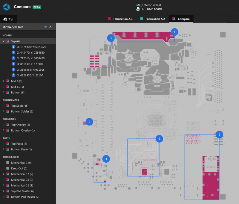
Gerber comparison becomes useful when an existing fabrication release provides a meaningful baseline. A footprint correction, connector relocation, or mask adjustment should produce explainable changes on identifiable layers. Comparing exported revisions helps reveal secondary changes that may be missed during native layout review, particularly after polygon repours or output configuration changes.
An effective comparison uses equivalent output settings and correctly matched layers between revisions. Engineers can inspect the visual differences against the approved change description, including layers expected to remain unchanged. Unexpected differences need investigation before release. For a first fabrication release, or a board that has been extensively redesigned, complete output inspection usually provides more value than interpreting a dense comparison against an unsuitable baseline.
The free Altium 365 Viewer supports browser inspection of Gerber artwork and corresponding NC drill files, regardless of which ECAD software was use to create the Gerber fileset. Gerber Compare accepts RS-274X and X2 datasets and displays layer differences with older geometry in red and newer geometry in green. Users can inspect each source dataset separately, navigate changes, and take measurements without installing software or registering.
Corrections found during review should then be applied to the source design and/or output configuration, and the output files will need to be regenerated and inspected again. Editing only the CAM artwork is normally performed by the CAM department at a manufacturer and those changes do not propagate back into the original CAD files. Make sure to keep a record of the required changes, approvals, and any further changes recommended by the PCB supplier so that the next revision incorporates the running record of required design updates.
When you need to quickly generate and publish Gerber files for your design and send your manufacturing documentation to your manufacturer, use the Altium Develop platform. No other design application provides a complete set of design, sharing, and PCB Gerber viewer features in a single application.
We have only scratched the surface of what is possible to do with Altium Designer on Altium 365. You can check the product page for a more in-depth feature description or one of the On-Demand Webinars.
Frequently Asked Questions
How do I inspect Gerber files before sending them to a PCB manufacturer?
Open the exact manufacturing package you intend to deliver and verify layer assignments, copper-layer order, board outline, and drill registration. Review each layer individually, then overlay related layers and measure suspect widths or clearances against the fabricator’s requirements. Where supported, CAM design-rule checks and netlist comparison provide additional verification beyond visual inspection.
How can I check whether my drill files align with my Gerber layers?
Import the NC drill files alongside the Gerbers and overlay the drill hits on the corresponding copper pads. Check hole centers, diameters, annular rings, and slot locations across several board regions. A consistent offset or scaling error warrants checking import units and coordinate settings; blind and buried vias also require correct drill-span assignments.
Which Gerber viewers support RS-274X and Gerber X2 files?
Altium Designer’s CAMtastic editor and the browser-based Altium 365 Viewer can display RS-274X and Gerber X2 manufacturing files. Altium 365 Gerber Compare also accepts both formats for revision comparison. X2 includes attributes describing layer and feature functions, although how those attributes are used depends on the viewer.
How do I view Gerber files in Altium Designer or Altium 365?
In Altium Designer, create a CAM document through File → New → CAM Document, then use File → Import → Quick Load to import the manufacturing files. Review the assigned layer types and physical order after import. In Altium 365, upload the Gerber and NC drill package to the standalone viewer, or save it to Personal Space for persistent access.

About Author
Related Resources
Related Technical Documentation
Table of Contents
Solutions for Every Role and Team
- Discover and evaluate design options earlier
- Develop in one shared workspace
- Scale with control and compliance
- Connect every stage of hardware development
Learn More
Thank you, you are now subscribed to updates.