


Propagation Delay Calculators in High-Speed PCB Design

At a Glance
You’ll need to make sure your signals are synchronized in your high speed PCB. Here’s how a propagation delay calculator in your design software can help.


Propagation delay is a property of any device or circuit that admits a traveling electromagnetic wave. It is most commonly associated with transmission lines on a PCB, where a signal is traveling at a definite speed. The wave speed is, of course, the speed of light, and the speed of light on any PCB interconnect is determined by the dielectric constant of the PCB materials and surrounding media.
In this guide, my goal is to discuss everything needed to understand propagation delay on transmission lines, including in vias that might appear on a transmission line. We care about this quantity for multiple reasons, principally for preventing timing mismatch on parallel buses involving single-ended or differential transmission lines, or both. In this guide, I will go over what propagation delay is and why we start to care about it so much in high-speed digital design.
Propagation Delay Defined
Propagation delay is the time required for a signal’s electromagnetic field to move along a transmission line from one point to another. In PCB interconnects, this delay is normally stated in ps/in, ps/mm, or as a total delay value between two points in the routed topology. Once the delay is known, it can be used for timing matching, length tuning, via delay compensation, and comparison against setup and hold timing requirements in a digital interface.
- Propagation delay depends on the effective dielectric constant seen by the signal, which is set by the trace geometry, reference plane arrangement, and surrounding dielectric materials.
- Propagation delay can be a function of frequency when dispersion is present, meaning different frequency components of the same signal travel at different velocities.
- Microstrip, stripline, coplanar waveguide, differential pairs, and vias can all have different propagation delays, even when they use the same laminate system.
- In simple calculators, propagation delay is often treated as a constant value, but high-speed channels require a frequency-dependent view once loss and dielectric dispersion become important.
Mathematically, for a quasi-TEM transmission line, propagation delay has a simple relation to the inductance and capacitance of a transmission line (units of time/length):

The actual equation is much more complicated because it is based on the lossy impedance, not the simple lossless impedance formula. Lossy impedance is a function of frequency, and it includes the loss tangent, skin effect resistance, DC resistance, and impact of copper roughness in the skin effect. When these terms are included, the propagation constant is:

Top: single-ended propagation delay, bottom: differential pair propagation delay.
While in principle it is possible to account for the k_g term here in terms of the lossless impedance, as I have shown in another article, modern CAD tools and EDA software do not actually solve this problem analytically. Instead, they use two possible methods:
- An empirical model developed from measurements or electromagnetic simulations is used to calculate propagation delay.
- The electromagnetic field in the interconnect is solved directly, and the propagation delay can be determined from the field solutions.
So that, in a nutshell, is how propagation delay is determined. In Altium Designer, this is performed in the Layer Stack Manager when you calculate the impedance on each layer. The propagation delay is needed for other important tasks in the high-speed design, specifically for length tuning/delay tuning in parallel buses and accounting for via delay or pin package delay in more specialized situations.
Simple Propagation Delay Calculation Without Dispersion
The simplest propagation delay calculators use the lossless impedance of a transmission line, as shown above. As long as trace impedance and capacitance/inductance are known, the propagation delay is also known. Because lossless impedance has no dispersion, the propagation delay will also have no dispersion, i.e., it will be the same at all frequencies.
There are also two formulas for single-ended microstrip and stripline propagation delay:

The Dk(eff) term in the microstrip equation comes from a famous result cited in Brian C. Wadell’s seminal textbook, titled Transmission Line Design Handbook. More complicated transmission lines, such as waveguide structures, differential structures, and coplanar ground structures, will have a different Dk_eff term defining the propagation delay.
Vias Without Dispersion
What about the propagation delay for vias?
Via propagation delay is difficult to determine because a via is not a uniform TEM or quasi-TEM transmission line in the same way as a trace over a reference plane. The signal current moves through a vertical conductor, but the return current must transition between reference planes through nearby plane capacitance, stitching vias, or some other return path structure. The electromagnetic field geometry changes along the via span, and the resulting delay depends on:
- Via drill diameter
- Antipad diameter
- Pad stack
- Reference plane spacing
- Unused via stub length
- Dielectric constants in the layer stack
- Return via arrangement
For this reason, via propagation delay is generally determined with a 3D electromagnetic field solver or extracted from S-parameters rather than calculated from a simple closed-form equation.
The dispersion in a via often does not become obvious until the frequency range rises above approximately 1 GHz because the via is electrically short at lower frequencies. When the signal wavelength is long compared with the physical dimensions of the via transition, the structure behaves more like a lumped discontinuity with some excess capacitance and inductance. The phase response then stops scaling linearly with frequency, and the via delay becomes frequency-dependent.
Propagation Delay With Dispersion
Remember that the propagation delay (for single-ended or differential signals) with all the lossy terms included is:
Top: single-ended propagation delay, bottom: differential pair propagation delay.
All of these lossy terms, as well as the dielectric constant, are functions of frequency. Therefore, the propagation delay is also a function of frequency. You can take tabulated data for the loss tangent and Dk, and calculate the skin effect with roughness, and this gives the transmission line impedance and propagation delay as a function of frequency. You can see some examples of dielectric constant variation over frequency in the resources below:
- Differences Between Prepreg Material vs. PCB Core: What Designers Need to Know
- How to Measure FR4 PCB Dielectric Constant
While propagation delay with dispersion can be calculated using the above formula, or the simpler delay formulas with varying Dk value, the typical approach is to calculate it from an insertion loss plot. The phase of the insertion loss plot allows the propagation delay to be calculated at each frequency value in the insertion loss plot. The formula used for this is:

Propagation delay calculation from insertion loss phase data
An example insertion loss plot with the phase overlay is shown below. In this plot, we can see the successive phase accumulation each time the phase resets to 180°. By applying a finite difference to the first derivative in the formula, we can get the second graph shown below, which is the propagation delay as a function of frequency.

If the dielectric constant had the same value at all frequencies, the propagation delay curve would be completely flat. Of course, this is not the case, and there will be losses in the interconnect as well. We can extract an effective Dk value as a function of frequency from this plot using the speed of light. This effective Dk value summarizes the total effects of dispersion in the dielectric constant, loss tangent, skin effect, and roughness.
While it is clear that propagation delay varies with frequency, why do we care about this in a practical sense? The reason becomes very important at very high channel bandwidth values, where digital signals are transferring data in the multi-Gbps range. At these ranges, dispersion causes the input digital signal to spread because different frequency components are moving faster than others. You start to notice this around 3 GHz, and it contributes to bit error rates when channel bandwidths are in the tens of GHz.
The resulting stretching of a signal reduces the edge rate. When taken with other effects like crosstalk, ISI, and reflections, these factors contribute to bit error rate as seen at the receiver. These effects can be seen in an eye diagram.

Calculating Via Propagation Delay
The propagation delay of a via can be quite complicated as a function of frequency. In other words, vias exhibit a lot of dispersion, and depending on the frequency range, this will distort the edge rate of signals traversing the via. All vias have these properties, but the frequency range where the impact is important depends on the via design.
Via propagation delay does not obey some simple formulas presented in textbooks, for example. I have highlighted this fact numerous times from Howard Johnson’s High-Speed Digital Design: A Handbook of Black Magic, which provides a model for via impedance and propagation delay. The author notes that the formulas are wrong in the frequency range where you actually observe strong dispersion in via impedance and propagation delay. Therefore, we also have to use the phase data from an insertion loss plot to determine the propagation delay through a via.

The insertion loss plot above is for a via in a six-layer PCB transitioning from L1 to L4, or an equivalent distance of 50 mil. From the plot, we see that the propagation delay is approximately 15 ps for a laminate system with Dk = 4. If we only used the speed of light to calculate the propagation delay, we would find the result is approximately 8.33 ps. Clearly, such simple calculations are inadequate in vias given the complex wave behavior in these structures.
If the via propagation delay is known, it can be assigned to a particular via in the Properties panel. Select the via, open the Properties panel, and enter the value in picoseconds.

Transmission Line Propagation Delay From S-Parameters
For a transmission line with measured or simulated S-parameters, propagation delay can be extracted from the phase of the insertion loss term. In a 2-port network, this is normally S21. In a differential channel, the same process is applied to the appropriate mixed-mode insertion loss term (SDD21). The insertion loss magnitude shows how much signal energy is lost versus frequency, while the phase shows the accumulated phase shift as the wave travels through the interconnect. The phase data is the quantity needed to calculate delay, just as we had above for vias.

Insertion loss curve (solid line) for a differential pair with phase overlay shown (dashed line).
An important part of the calculation is to select the right phase data. The phase plots are normally bounded between +180° and -180° because the phase accumulates with a period of 360°, so the phase resets each time the accumulated phase passes one of these limits. Unwrapping refers to removing these artificial discontinuities so that you have a continuous phase curve. Once the continuous phase is available, the delay can be calculated from the slope of phase versus angular frequency.
The propagation delay plot will normally show some amount of dispersion. This dispersion is due to the natural variation of dielectric constant with frequency, as well as all frequency-dependent losses in the transmission line. Loss tangent, skin effect, copper roughness, and current redistribution all affect the phase response, so the extracted propagation delay becomes a practical summary of how the channel changes the timing of different spectral components in the signal.
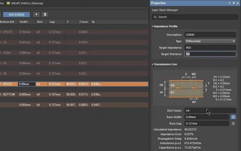
Lossless Transmission Line Propagation Delay From Your Layer Stack
A lossless transmission line propagation delay can be calculated directly from your layer stack using the Layer Stack Manager in Altium Designer. When impedance is calculated for a specific routing layer and geometry, the tool can also report the propagation delay based on the stackup materials, dielectric thicknesses, copper arrangement, and trace width.
This value is only a lossless propagation delay, so it does not include the full frequency-dependent behavior from loss tangent, skin effect, roughness, and dielectric dispersion. Even with that limitation, it is a good estimate of the actual propagation delay in a low-loss transmission line, and it is usually accurate enough for initial length matching, delay tuning, and timing-budget setup before a more detailed field-solver or S-parameter analysis is performed.
Whether you need to build reliable power electronics or advanced digital systems, use Altium’s complete set of PCB design features and world-class CAD tools. Altium provides the world’s premier electronic product development platform, complete with the industry’s best PCB design tools and cross-disciplinary collaboration features for advanced design teams. Contact an expert at Altium today!
Frequently Asked Questions
What determines propagation delay in a PCB transmission line?
Propagation delay is primarily determined by the effective dielectric constant seen by the signal. Trace geometry, reference plane spacing, routing layer, dielectric material, solder mask, and nearby copper all influence the effective dielectric constant.
Why does microstrip propagation delay differ from stripline propagation delay?
Microstrip fields travel through both dielectric material and air or solder mask, while stripline fields are mostly confined inside the dielectric. The effective dielectric constant for a microstrip is always lower than the bulk dielectric constant, so the microstrip propagation delay is always faster.
How do you calculate propagation delay from a PCB layer stack?
A lossless estimate can be calculated from the stackup using the trace geometry, dielectric thickness, copper arrangement, and material dielectric constant. CAD tools such as Altium Designer can report this delay when impedance is calculated in the Layer Stack Manager.

About Author
Related Resources
Related Technical Documentation
Table of Contents
- Propagation Delay Defined
- Simple Propagation Delay Calculation Without Dispersion
- Vias Without Dispersion
- Propagation Delay With Dispersion
- Calculating Via Propagation Delay
- Transmission Line Propagation Delay From S-Parameters
- Lossless Transmission Line Propagation Delay From Your Layer Stack
- Frequently Asked Questions
Design to Release, Without the Friction
- Keep reviews tied to the right version
- Reduce handoff confusion and rework
- Spot sourcing and release risk earlier
- Work solo, share when needed
Get Started
Thank you, you are now subscribed to updates.

