


High-Speed PCB Design Tips and Guidelines

At a Glance
Essential tips for high-speed PCB designs, and when you need to start being concerned about how and where you route your traces.


In this article, we’ll examine a few tips and guidelines for high-speed printed circuit board designs.
When it comes to high-speed designs, we are typically concerned with two areas. The first of them is signal integrity (SI), and issues related to crosstalk due to trace spacing, reflections due to impedance mismatches, attenuation of the signal, and problems such as ringing. Of course, we would like to minimize those problems to the best of our ability. Secondly, we are concerned with electromagnetic interference (EMI).
Before we get started, I have to recommend a fantastic video on Altium’s YouTube channel by Rick Hartley on proper PCB design and how to achieve proper grounding. The topics covered in detail in that video are especially important for high-speed digital and high-speed analogue designs.
What Is a "High Speed" PCB design?
Before we get into these high-speed PCB design and layout tips, let's take a look at when we actually have to care about all of this!
Let's say, for example, that we have a 100 MHz clock signal in our design, and naively assume this to be the highest frequency apparent in our system. It turns out that the problem is not actually that the clock signal has a fundamental frequency of 100 MHz but rather that our design issues come from the rise and the fall times of this near square-wave clock signal.
These sharp transitions going from digital low to digital high (or vice-versa) contain far higher frequency content than the fundamental. Given a signal’s rise and fall times (depending on which of them is faster), we can calculate the maximum frequency within the signal (or rather the bandwidth) approximately using the following formula:

For example, for a 100 MHz clock signal with a 1 ns rise time, the bandwidth of that signal is 500 MHz—quite a significant difference!
When a PCB trace length exceeds 1/12th of the wavelength in the dielectric, we need to start considering our PCB design in far more detail. This is the point when our traces start to look like distributed length transmission lines, and not like lumped elements anymore. We call this length the “critical length.”
Tip #1: Reference Planes
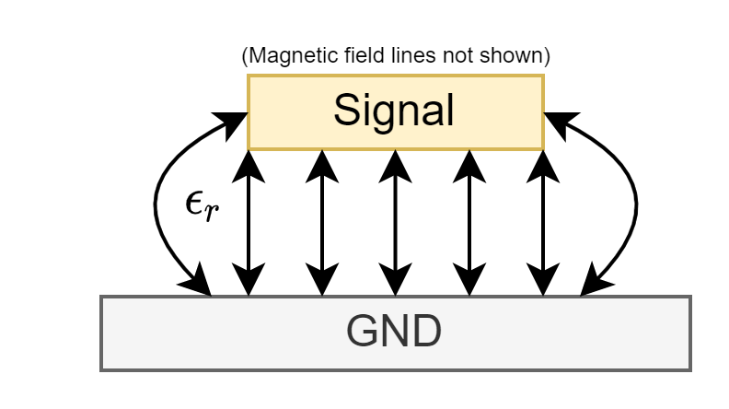
We always want to have a ground or relevant power plane adjacent to a signal plane, directly on the layer below (or above) a layer carrying a trace. In certain cases, you can use a relevant power plane instead of a ground plane as a reference. Relevant here means that the reference plane voltage is the same voltage as the signal is derived from. Reference planes are not only important to maintain proper return paths and to minimize electromagnetic field spread, but also when requiring controlled-impedance traces.
For AC signals, anything above a few kHz, and the return path is actually directly below the signal trace in the reference plane below. A very important rule is that there should be no splits in the reference plane underneath traces.
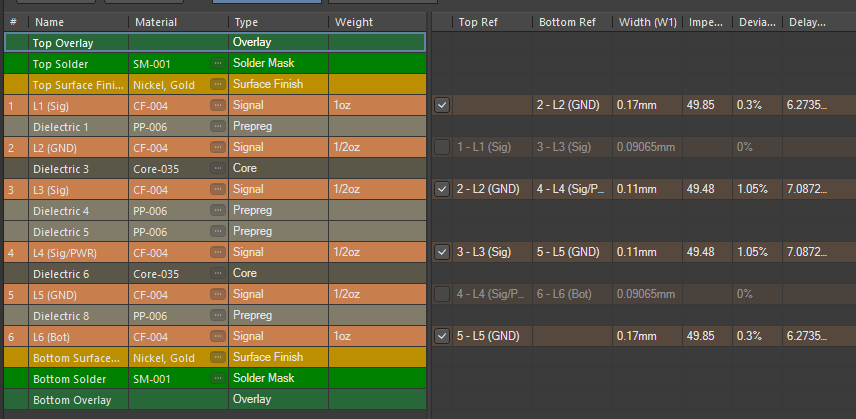
Tip #2: Board Stack-Up
We want to have a ground plane not only adjacent to a signal plane but also adjacent to a power plane. It is also a good idea to have a thin dielectric between planes, which in turn gives us tight coupling and also allows us to use thinner traces for denser designs.
Thinner traces additionally give us more space to work with, and more space between traces. However, keep in mind that the manufacturing of thin traces can be more difficult.
Tip #3: Controlled Impedance Traces
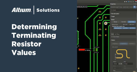
As soon as our trace length exceeds the critical length discussed in the introduction of this article, we need to control the impedance of our traces. That is, we need to adjust the width of our trace—depending on our chosen PCB stackup and build-up—to give us a certain transmission line impedance. Typically, this will be 50 Ohms for single-ended signals. Altium Designer, available within Altium Develop, features a powerful 2D field solver that can calculate the required trace widths depending on your stackup and build-up for you in seconds!
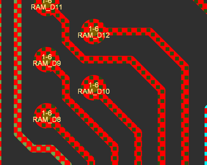
Tip #4: Trace Length, Spacing, and the 3h Rule
We need to keep high-speed traces as short as possible—this helps with EMI and SI. Additionally, we want to keep different high-speed traces as far away from each other as possible to minimise crosstalk.
Additionally, aim to keep high-speed traces away from components such as inductors or power sections of a circuit. A typical rule of thumb is the 3h rule, which means the traces should be separated by at least three times the height of the dielectric between the signal layer and the next ground or reference layer.
For high-performance, high-speed designs, we often require simulation tools to verify that we are meeting required signal integrity and EMI performances.
Whether you need to build reliable power electronics or advanced digital systems, Altium Develop unites every discipline into one collaborative force. Free from silos. Free from limits. It’s where engineers, designers, and innovators work as one to create without constraints. Experience Altium Develop today!

About Author
Related Resources
Related Technical Documentation
Table of Contents
Design to Release, Without the Friction
- Keep reviews tied to the right version
- Reduce handoff confusion and rework
- Spot sourcing and release risk earlier
- Work solo, share when needed
Get Started
Thank you, you are now subscribed to updates.