Signal Integrity Principles based on Altium Designer 24

Introduction to High-Speed and Signal Integrity
Digital systems are one of the fundamental areas of modern electronics. The advancement in highly efficient processors or other digital systems, like FPGAs or wide-bandwidth data acquisition systems that use fast ADCs converters together with DSPs or FPGAs, requires a different approach to electronic design, especially PCB that includes interconnects between various integrated circuits or modules. This approach is related to the types of signals used in modern, high-speed electronics.
Basic and well known interfaces, such as RS232 or I2C, are limited in data throughput to hundreds of kilobits per second, however interconnects between high-speed systems or modules via interfaces such as PCIe or USB3.0 may have data rates above gigabits per second (and hence the term high-speed systems or high-speed design).
In addition, most of the modern high data rate interconnects use serial signaling with only a few signal lines. One such serial line is shown in figure 1. Some standards require multiple lines and in most cases those lines are made as a differential pair. A good example of such standards are PCIe or JESD204.

Figure 1: Serial high data rate link; please note the impedance matching of the transmitter, receiver and transmission line is fundamental for signal integrity
Principles of high-speed designs are similar to radio frequency designs as there is a direct relationship between the signal data rate and the bandwidth occupied by this signal - the higher the data rate, the wider the bandwidth occupied by such signal. Also, rise and fall time of the high-speed signals are often below 1ns often with switching frequencies above a few GHz. Such signals propagate through PCB in a different way than signals used in low speed standards, like SPI, I2C or RS232. Significant attention is required to design the PCB correctly, keeping in mind the bandwidth of the signal, so that the fidelity of the data link is maintained starting from the transmitter (e.g. JESD204B interface of an ADC) to the receiver (e.g. FPGA input pins). Most often the LVDS (low-voltage differential signaling) standard is used to interconnect high data rate modules or systems as well as to provide a standardized specification for high-speed signals (e.g voltage swings, logic levels, impedances and more).
The nature of the high-speed signals requires different design tools for the PCB and schematics to ensure high fidelity of the link and signals transmitted on the PCB (together with time reduction spent on the design). High fidelity of the signal related to quality characteristics is called the signal integrity, which consists of a number of parameters of the transmitted signal that can be verified during the PCB/SCH development as well as in the lab by signal measurements with dedicated tools.
Altium Designer supports all activities related with high-speed projects and provides means of control over the signal integrity by providing a number of features, for example:
- possibility to define differential pairs in the schematics and PCB;
- routing of the differential pairs in the PCB editor with length matching;
- definition of controlled impedance tracks for differential and single-ended signal lines;
- signal lines length tuning within a differential pair as well as within a bus;
- simulation tools and DRC check for signal integrity and high-speed;
- possibility to define PCB stackup with impedance profiles that include dissipation factor, dielectric constant and copper roughness;
- possibility to define propagation delays for components
and more.
These features help to mitigate design errors related to signal integrity, provide flexibility in the design phase, reduce prototyping costs, and accelerate product delivery to the market.
Signal Integrity
The signal degradation mentioned in the first paragraph may take various forms and refer to time related values of the signal (like rise time or jitter) or parameters related with signal level (e.g. overshoot, voltage swing). The basic parameters related with signal fidelity includes the following phenomenons:
- signal reflections between the signal transmitter and the transmission line (or receiver and the transmission line), as well as signal reflections caused by connectors, vias, stubs or other components of the system that distorts the impedance continuity along the signal path;
- crosstalk between signal lines;
- over- and undershoot of the signal;
- degradation in the signal to noise ratio (caused by the coupled noise), causing difficulties for the receiver to detect the correct logic levels;
- signal attenuation along the signal path- inability to achieve the required logic levels;
- jitter on the clock signal that sets the operation of the ADC/DAC converters as well as the jitter of the signal lines;
- increased levels of radiated emission from the PCB (or the system) that may require various countermeasures (e.g. shielding) in order to pass EMC certification
and more.
Each of the phenomena listed above may lead to increased data error rate or complete loss of communication. Also, deterioration of the system parameters (e.g. the quality of signal processing through high resolution ADC converters) may occur as well. Examples of signal disturbances related with poor design are shown in oscillograms and simulations performed in AD24 - see figures 2 to 5.

Figure 2: Runt pulses caused by improper signal termination along the signal path

Figure 3: Crosstalk example - purple trace - aggressor, yellow trace - victim

Figure 4: Over- and undershoot of the digital waveform

Figure 5: Signal ringing example. Signal integrity simulation result performed in AD24

Figure 6: Optimisation in signal ringing - series termination resistor sweep
Single Ended and Differential Signals
Low-speed signals such as SPI, I2C or RS232, where information is carried as the voltage difference between the signal line and ground, are called single-ended signals. High-speed signals, with data rates exceeding several hundred Mbits/s are usually transmitted by the differential pair - a closely coupled pair of signal traces on the PCB - the information in this case is carried by the voltage difference between these two lines (often referred to as P and N) - see figure 7 and 8.

Figure 7: Differential pairs of the Ethernet controller defined in AD24

Figure 8: Differential pair represented on the PCB
Differential signals are less susceptible to disturbances and fluctuations in the ground potential on the PCB because a disturbance is induced in both lines that form a differential pair, thus the differential signal (difference between one line and the other) is not distorted. This type of signaling helps to minimize problems related to ground bounce in the system and improves the quality parameters of high-speed signals. Examples of differential and single ended signals are shown in figure 9.

Figure 9: Single Ended and Differential signals
Conclusions
Correct implementation of a high-speed principles in the project to ensure the integrity of signals on the PCB requires attention from the beginning of the design stage - starting from the PCB stackup, definition of the differential or single-ended pairs with correct impedances, routing strategies as well as arranging the components on the PCB, e.g. the location of DDR memory and the with respect to MCU or FPGA.
In addition, important aspects related to the quality of high-speed signals include type and count of vias along the signal paths, signal stubs, connectors and the method of connecting signal traces to them.
Verification of a manufactured PCB with high-speed signaling can be performed through simulation, which allows you to detect potential problems before ordering it. Signal integrity criteria such as overshoot, undershoot, reflection or crosstalk can be defined in Altium Designer in the design rules. This helps to keep the signal-integrity under control.
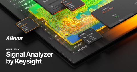
Our upcoming extension, Signal Analyzer by Keysight, will further enhance the potential of your design process, especially when focusing on signal integrity analysis. The premiere of this extension is scheduled for mid-October 2024.


