


USB High Speed (ULPI) Routing

At a Glance
Learn what ULPI is for USB High Speed interfaces, as well as best practices for routing this bus on a PCB.


There are many variants of USB on the market today, ranging from variations of the protocol itself to variations within the protocol. In this article, we’ll be examining the ULPI (UTMI+ low pin interface) interface, which can be found in USB high speed (HS) PHYs.
In comparison to the UTMI+ specification and interface, as the name implies, ULPI is a low pin-count variation of this bus. This helps us as PCB design engineers, as we do not need route out and length-match as many tracks. This is beneficial for space-constrained designs, as well as for EMI reasons.
ULPI is a high-speed interfacing, allowing the final USB HS implementation to achieve a specific maximum bitrate of 480 Mbps. We therefore need to be careful with routing to avoid EMI and SI issues.
For a more in-depth look, make sure to check out this video.
ULPI Basics
A USB HS PHY is - very simply put - a transition point between a ULPI interface and a USB differential pair that a USB connector sees. The ULPI interface is exposed to a compatible IC, such as an advanced microcontroller, FPGA, or System on Chip (SoC).
The ULPI interface is composed of an 8-bit wide, bi-directional data bus (DATA[7:0]), a clock signal (CLK) running at a frequency of 60 MHz, and various control signals (DIR, STP, NXT).
Rise and Fall Times
Although the clock frequency at 60 Mhz may seem low, we need to remind ourselves that we aren’t necessarily concerned about the clock frequency, but rather the rise and fall times.
This is due to the fact that those edges of our digital (nearly) square wave signal contain the majority of the high-frequency information. Without detailed analysis, this is easily seen by looking at the fourier series of a square wave, which is composed of the fundamental (in our case, 60 MHz), and odd harmonics extending out to infinity with decreasing power levels.
Unfortunately, rise and fall times are usually difficult to find on a manufacturer’s datasheet and need to be extracted via IBIS files. Datasheets typically only give us a ‘best case’ for rise and fall times - something that isn’t entirely useful.
In any case, due to this high-frequency harmonic content, as well as the timing constraints imposed by the ULPI interface, we need to take care when routing.
Controlled Impedance
ULPI signals require impedance control, as at the frequencies concerned, and for longer traces, the traces will act as transmission lines. Thus, the impedance needs to be matched to the driver and receiver.
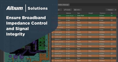
Typically, we require ULPI traces to be 50 Ohms controlled impedance. Impedance calculation for traces is not a part of this article, however, Altium Designer has a very hand 2D field solver built-in.
You’ll need to know your PCB build-up and enter this information into Altium Designer’s ‘Layer Stack Manager’. Then, you can navigate to the ‘Impedance’ tab and let Altium Designer calculate the required trace width for a given impedance.

As a short aside, the USB high-speed differential pair needs to be routed with 90 Ohms differential impedance.
Delay Matching

Apart from controlling our trace impedance, we also need to delay-match the traces. The ULPI specification, in combination with the PHY datasheet’s timing specifications, can be used to determine the timing budget.
If you haven’t calculated timing budgets before, make sure to check out Xilinx’s user guide UG863 and in particular the USB2.0 section. This will give you the calculations for maximum allowed trace length, as well as maximum delay variations between ULPI signal traces and the CLK trace.
In any delay-matching scenario, remember to take into account pin delays of your controller’s package. Pin and package delays, as was the case with rise and fall times, can be quite hard to come by at times. However, these package delays can be in the order of 100s of picoseconds, which can throw off your timing budget in certain cases.
In addition, via delay needs to be accounted for. An easy routing method that allows you to ignore via delay, is to route all traces equally. In essence, this means use the same number of vias and same layer transitions for all ULPI signals.
Reference Planes
Remember to have solid reference planes (preferably, ‘0V’ planes) directly adjacent to your signal traces. Preferably, with a thin dielectric in between. Also, do not route ULPI traces over splits or voids in the reference plane.

Lastly, whenever transitioning between references and layers with a signal via, make sure to place a ‘transition’ via (at ‘0V’) close to the signal via. This makes sure that during the Z-axis transition, the return path is still well defined and ensures a good reference plane transition.

ULPI routing requires attention when it comes to PCB layout and routing. However, with some thought and following the guidelines in this article, you too can create working ULPI designs while avoiding EMI and SI issues.
Altium Designer can help you along the way, with its advanced 2D field solver for impedance calculations, as well as delay and length matching tools.

About Author
Related Resources
Related Technical Documentation
Design to Release, Without the Friction
- Keep reviews tied to the right version
- Reduce handoff confusion and rework
- Spot sourcing and release risk earlier
- Work solo, share when needed
Get Started
Thank you, you are now subscribed to updates.