Skip to main content
Mobile menu
PCB Design
Altium Designer
World’s Most Popular PCB Design Software
CircuitStudio
Entry Level, Professional PCB Design Tool
CircuitMaker
Free PCB design for makers, open source and non-profits
Why Switch to Altium
See why and how to switch to Altium from other PCB design tools
Solutions
For Enterprise
The Last Mile of Digital Transformation
For Parts and Data
Extensive, Easy-to-Use Search Engine for Electronic Parts
Altium 365
Resources & Support
Explore Products
Free Trials
Downloads
Extensions
Free Altium 365 Tools
Online PCB Viewer
Resources & Support
Altium / Renesas Scheme: Information for Shareholders
All Resources
Support Center
Documentation
Altium Community
Forum
Bug Crunch
Ideas
Education Programs
Professional Training / Certification
University / College Educators
University / College Students
Webinars
Store
Search Open
Search
Search Close
Sign In
PCB Routing
Main menu
Home
PCB Design
Collaboration
Component Creation
Data Management
Design Outputs
ECAD/MCAD
HDI Design
High Speed Design
Multi-Board
PCB Layout
PCB Routing
PCB Supply Chain
Power Integrity
RF Design
Rigid Flex
Schematic Capture
Signal Integrity
Simulation
Software
Altium 365
Altium Designer
Enterprise Solutions
PDN Analyzer
Upverter
Education
Programs
Altium Academy
Engineering News
Guide Books
Newsletters
Podcasts
Projects
Training Courses
Webinars
Whitepapers
FREE TRIALS
Best in Class Interactive Routing
Reduce manual routing time for even the most complex projects.
Explore Solutions
PCB Routing
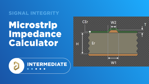
Microstrip Impedance Calculator
Learn more about using and interpreting results from a microstrip impedance calculator.
Read Article
Altium Live Question: Digital Signals in a Grounded Coplanar Waveguide?
Have you considered the effects of a GPCW structure on digital signals? Here’s a hint: look at the S-parameters!
Read Article
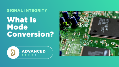
A Guide to Mode Conversion, Its Causes, and Solutions
Differential pairs are most often discussed in terms of their impedance and length matching tolerance, both with the goal of ensuring proper termination at the receiver and suppression of common mode noise. On interconnects, such as board-to-board connections or cascaded transmission line arrangements, you have an important EMC compliance metric that is sometimes overlooked. This is mode conversion, which can be visualized in an S-parameter
Read Article
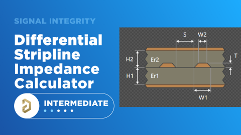
Differential Stripline Impedance Calculator
Try our differential stripline impedance calculator, built based on Wadell’s equations.
Read Article
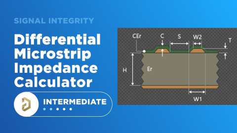
Differential Microstrip Impedance Calculator
Learn more about using and interpreting results from a differential microstrip impedance calculator.
Read Article
Differential Pair Impedance: Using a Calculator to Design Your PCB
Do you know what to look for in your differential pair impedance calculator? We've compiled the important information you need to know in this short guide.
Read Article
PCB Via Size and Pad Size Guidelines
Do you know what PCB via size you should use in your PCB layout? We’ll look at a few simple ways to answer this question.
Read Article
When to Use Tented Vias in Your PCB Layout
Some designers swear by tented vias and prefer to always use them. When should these be used and when should they be avoided? We’ll explore in this article.
Read Article
What's HDI? Design Basics and the HDI PCB Manufacturing Process
Learn about design basics for HDI PCB board design. When planning for the HDI PCB manufacturing process, you can prepare accurate designs and deliverables with Altium Designer.
Read Article
Recover Conductor Losses By Clearing Your PCB Ground Layer
Need to recover some conductor losses? Here’s how clearing out your ground plane near an I/O or connector can help.
Read Article
How to Design to a Differential Impedance Specification
Differential impedance is sometimes misunderstood and it depends on multiple factors. Learn more about trace width design needed to reach a specific differential impedance target.
Read Article
Should You Use Tight vs. Loose Differential Pair Spacing and Coupling?
We get a lot of questions about trace impedance and how to calculate the right trace size to hit a specific impedance in a manufacturable PCB. Just as important as determining an appropriate trace width for a single-ended trace is determination of an appropriate spacing between two traces in a differential pair. So the question is, how close do the traces in a differential pair need to be to each other, and is the need for “tight coupling” really
Read Article
Routing Requirements for a USB Interface on a 2-Layer PCB
In an earlier blog , I discussed some of the basic points in preparing routing rules for 2-layer PCBs to support routing and layout with digital signals. In particular, we looked at some of the basic stackup and routing rules needed to support a digital interface like I2C or SPI on a 2-layer PCB. When working with these interfaces, a few simple guidelines can help ensure signal integrity in your board and cut down on EMI. What about an impedance
Read Article
Can You Route Digital Signals on a 2-layer PCB Design?
2-layer PCBs are a common entry-level choice for designers, and they can even support high speed designs if built correctly.
Read Article
Two 4 Layer PCB Stackups With 50 Ohms Impedance
Need a 4-layer PCB stackup that can support high speed components on both sides of the board? Consider these alternatives to the typical 4-layer stackup.
Read Article
Microstrip PCB Ground Clearance Part 2: How Clearance Affects Losses
In a previous article, I provided a discussion and some simulation results on the necessary clearance between impedance controlled traces and nearby grounded copper pour. What we found was that, once the spacing between the pour and the trace becomes too small, the trace becomes an impedance-controlled coplanar waveguide (with or without ground). We also saw that the 3W rule for the spacing between the trace and the grounded copper pour is a bit
Read Article
What Are Differential Pairs and Differential Signals?
Differential pairs and differential signaling are the mainstay of high speed digital communication and data transfer.
Read Article
Pagination
First page
« First
Previous page
‹‹
Page
3
Current page
4
Page
5
Page
6
Page
7
Page
8
Next page
››
Last page
Last »
Load More